COMPANY PROFILE / SEMICONDUCTOR BACK-END
SK hynix
The company that goes inside the advanced package has started building back-end plants of its own
SK hynix makes DRAM and NAND flash, and nothing else. Its name comes up in any discussion of AI silicon because it supplies HBM, high bandwidth memory, and HBM is the part that gets built into an advanced package such as TSMC's CoWoS. By origin, then, this is a company that gets let into the back end. Yet it is now putting up advanced packaging plants of its own, in Korea and in the United States. This profile traces what is happening, using only the figures the company has published.
Several Korean semiconductor companies carry the Samsung or SK name, and in any discussion of the back end three of them tend to appear at once. All three are separate legal entities, with different owners and different businesses.
1. SK hynix (the subject of this profile) = a memory specialist belonging to the SK Group. A leading supplier of HBM, and therefore the party that goes inside the advanced package. It is not part of the Samsung Group.
2. Samsung Electronics = an IDM with memory, logic and a foundry. It competes with SK hynix in memory and in HBM, and with TSMC in foundry work.
3. Samsung Electro-Mechanics = an electronic components maker that produces package substrates such as FC-BGA, and MLCCs. It is a separately listed company, distinct from Samsung Electronics.
Companies 1 and 2 are competitors; companies 2 and 3 are different companies inside the same Samsung Group. This profile deals only with company 1.
- SK hynix in 30 seconds
- The logo and how the name is written
- What the company actually does: the memory-only business model
- Scale: five years of revenue
- Company category and position in the back-end industry
- Sites and the countries where it manufactures
- Leading products and share in semiconductor back-end work
- Current investment plans
- Major corporate partners
- Where the company is heading in this field
- The risks this company carries
- Glossary, references and claim-to-source audit
1. SK hynix in 30 seconds
Nasdaq SKHY (July 2026)American Depositary Shares were listed on Nasdaq in July 2026
(memory only)Makes DRAM and NAND alone; runs no contract logic manufacturing
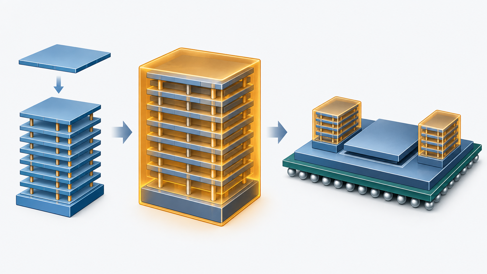
SK hynix is neither a foundry nor an OSAT. It is a specialist that makes only its own branded memory Sourced. It is treated as a leading player in the back end all the same, because of what HBM is as a product. HBM is DRAM stacked many layers high and wired together through electrodes that pass straight through the silicon, the TSVs, so stacking, connecting and encapsulating are the steps that decide what the product is worth. In HBM, in other words, the back end is the core of the product, not an appendage to the front end. The company itself names investment in advanced manufacturing equipment and in advanced packaging lines as the source of its competitiveness in HBM Sourced.
2. The logo and how the name is written
The SK hynix logo is a registered trademark of the company.
A note on style: the legal name is SK hynix Inc., with SK in capitals and hynix in lower case. Forms such as "SK Hynix" appear widely, but the company's own statutory documents use SK hynix without exception. SK is the group brand; SK square, the group's holding company, held 20.5% of the shares as of 31 March 2026.
Official site: https://www.skhynix.com/3. What the company actually does: the memory-only business model
Semiconductor companies come in three broad shapes, and SK hynix fits none of them exactly.
| Model | Design | Manufacturing | In this company's case |
|---|---|---|---|
| IDM (vertically integrated) | In house | In house | Yes, except that it makes only memory |
| Fabless | In house | Outsourced | No |
| Foundry | None | Contract | No. It runs no contract logic manufacturing business |
Precisely, it is a memory-only IDM. There are two products, DRAM and NAND flash, and in 2025 DRAM was 77.1% of revenue and NAND 21.3% Our calculation. The remaining 1.6% is an "other" line covering image sensors, some contract manufacturing and lease income.
The corporate history is convoluted. In 1983 the predecessor company built its first plant at Icheon and entered the memory business; it listed on the Korea Exchange in December 1996; in May 1999 it acquired the semiconductor memory business of the LG group; in March 2001 it was renamed Hynix Semiconductor; in February 2012 SK Telecom acquired it, and the following month it became SK hynix Inc. Sourced.
In July 2026 SK hynix listed American Depositary Shares on Nasdaq, under the ticker SKHY. The offer price was US$149.00 per ADS, covering the equivalent of 17,790,000 shares, and net proceeds were about US$26.2bn Sourced. With that, the company became subject to statutory disclosure in the United States. The prospectus this article relies on as primary material, Form 424B4, was filed for that offering, and it describes the plants, the customers and the procurement risks in unusual detail for a Korean company.
The use of proceeds is spelled out too: KRW 45.5tn for production facilities in Korea and about KRW 11.9tn for EUV lithography tools. How much of that flows towards the back end, meaning the advanced packaging plants, is the subject of section 8.
The company's own glossary defines the two technologies that hold HBM together Sourced. One is TSV packaging technology, described as a packaging technology that opens fine holes through the silicon and joins stacked chips to one another with vertical electrodes. The other is MR-MUF, mass reflow molded underfill, defined as a step that injects a liquid protective material into the gaps between stacked chips and cures it to protect the circuitry, with better heat dissipation than sandwiching a film between each chip.
Read from the materials side, that is a fork in the road. Do you put a film between the chips, or pour in a liquid resin and cure it? The answer decides what the market looks like for a materials supplier. That the company bothered to put MR-MUF in its statutory filing as a definition, and went on to compare it with the film approach on heat dissipation, suggests management regards the choice of stacking material as part of its competitive position.
4. Scale: five years of revenue
| Year | Revenue (KRW tn) | Operating profit (KRW tn) | Operating margin |
|---|---|---|---|
| 2021 | 42.998 | 12.410 | 29% |
| 2022 | 44.648 | 7.007 | 16% |
| 2023 | 32.766 | -7.73 | -24% |
| 2024 | 66.193 | 23.467 | 35% |
| 2025 | 97.147 | 47.206 | 49% |
The margins are the figures the company gave in each year's earnings release. The 35% for 2024 is derived from revenue of KRW 66.193tn and operating profit of KRW 23.467tn Our calculation.
Research and development, and capital expenditure
| Item | 2023 | 2024 | 2025 | Jan to Mar 2026 |
|---|---|---|---|---|
| R&D expense | KRW 3.751tn | KRW 4.436tn | KRW 6.466tn | KRW 2.451tn |
| Capital expenditure | KRW 8.325tn | KRW 15.946tn | KRW 27.519tn | KRW 7.657tn |
| Capex as a share of revenue | 25.4% | 24.1% | 28.3% | 14.6% |
R&D expense is stated after adjusting for development costs taken to the balance sheet. Capital expenditure is the cash outflow for purchases of property, plant and equipment. The capex ratios are ours Our calculation. The company states a capital allocation policy of holding capex to revenue in the mid-thirties per cent on a three-year rolling average, and says plainly that 2026 spending will be well above 2025.
What the 47,639 employees represent
At 31 March 2026 there were 47,639 permanent employees on a consolidated basis, and 35,929 at the parent company Sourced. Unusually, the company breaks the number down by region.
| Region | People | Share of the total |
|---|---|---|
| Korea | 35,321 | 74.1% |
| China | 11,333 | 23.8% |
| United States | 591 | 1.2% |
| Consolidated total | 47,639 | 100% |
The percentages are ours Our calculation. Korea, China and the United States add to 47,245, and the 394 difference against the consolidated total is presumably staff elsewhere, but the company gives no breakdown. It also states that it operates a profit-sharing incentive scheme funded by 10% of operating profit.
5. Company category and position in the back-end industry
The category is a manufacturer, a memory-only IDM. It takes no back-end work on contract, but it does assemble and test its own products in its own plants. The revenue split shows where the back end sits inside this company.
DRAM revenue of KRW 74.9tn is not an HBM figure. It also takes in DDR5 for servers, LPDDR for mobile devices and GDDR7 for graphics. It is useful anyway, because it fixes the ceiling on SK hynix HBM revenue.
What matters more from a back-end point of view is that the assembly and test plants belong to the company. As is usual for memory makers, SK hynix does not send back-end work to an OSAT; it runs its own assembly and test sites at Icheon and Cheongju in Korea and at Chongqing in China Sourced. With a product like HBM, where stacking and encapsulation decide what the part is worth, those steps cannot be handed outside.
6. Sites and the countries where it manufactures
Plants sit in two countries, Korea and China, or three once the site under construction in the United States is counted Sourced. Front-end wafer manufacturing and back-end assembly and test are separated out below.
| Country | Site | Process stage | Detail |
|---|---|---|---|
| Korea | Icheon | Front end and back end | Head office. DRAM fabs M10 (2005), M14 (2015) and M16 (2021), with assembly and test alongside them |
| Korea | Cheongju | Front end and back end | NAND fabs M11 (2008), M12 (2012) and M15 (2018). The clean room of M15X, an additional fab for HBM and high-performance DRAM, opened in October 2025. The advanced packaging plant P&T7 is under construction |
| Korea | Yongin | Front end (under construction) | An integrated campus of next-generation fabs and R&D facilities. Ground was broken on the first fab in February 2025, with the phase one clean room due in the first quarter of 2027 |
| China | Wuxi | Front end, plus back end through a joint venture | DRAM fabs C2 (2006) and C2F (2019). Back-end work uses the plant of the joint venture HITECH Semiconductor, established in November 2009, in which SK hynix holds 45.0% |
| China | Dalian | Front end | A NAND fab, acquired from Intel in December 2021 |
| China | Chongqing | Back end | The company's own assembly and test site |
| United States | West Lafayette, Indiana | Back end (under construction) | The first production site in the United States, dedicated to advanced packaging of HBM for AI. The first clean room is due to run in the second half of 2028, with a research and reliability centre alongside it |
The company states that every plant runs flat out, 24 hours a day and 365 days a year, on three shifts of eight hours.
As the table shows, SK hynix says plainly in its statutory filing which sites are front end and which are back end: that it owns and operates assembly and test facilities at Icheon and Cheongju in Korea and at Chongqing in China for the back-end processing of its own products. That degree of specificity is hard to find in a peer's disclosure.
For a materials supplier the difference is immediately practical. When the assembly and test sites are named, you can plan where encapsulants and bonding materials go, and how they get there. And because the new Indiana plant is described as dedicated to advanced packaging of HBM for AI, the fact that a destination for stacking materials will exist in North America from 2028 can now be read straight off a primary source.
7. Leading products and share in semiconductor back-end work
The product: HBM, and how it is built
SK hynix is bound up with the back end because of what HBM is, structurally. The company's own glossary definitions are set out here as written Sourced.
- HBM
- High Bandwidth Memory. Several DRAM dies stacked vertically and joined by TSV packaging technology, giving far more bandwidth than conventional DRAM. It sits next to an AI accelerator.
- TSV packaging technology
- Through-Silicon Via. A packaging technology that opens fine holes through the silicon and joins the chip above to the chip below with vertical electrodes. HBM stacking rests on it.
- MR-MUF
- Mass Reflow Molded Underfill. A step that injects a liquid protective material into the gaps between stacked chips and cures it to protect the circuitry. The company says it dissipates heat better than sandwiching a film between each chip.
- Custom HBM
- HBM configured to a customer's requirements, with some GPU or ASIC functions folded into the base die, the logic chip at the bottom of the stack. The company names this as a point of differentiation.
On its competitiveness in HBM, the company points to having been the first to develop HBM using TSV packaging technology, and to investment in advanced manufacturing equipment and advanced packaging lines sustaining volume while meeting customers' demanding quality requirements Sourced. HBM3E was commercialised in 2024 and HBM4 developed in 2025; in September 2025 the company says it became the first in the industry to complete preparations for HBM4 volume production.
On market share, plainly
SK hynix discloses neither HBM revenue on its own nor revenue from the packaging step. What is published stops at a qualitative statement that HBM revenue more than doubled year on year in 2025 Not yet confirmed.
The prospectus filed with the U.S. SEC does carry an HBM market share figure, but the text itself attributes it to an estimate by the research firm IDC. Appearing in a statutory filing does not make an outside estimate a primary source, so this article does not use that number Not yet confirmed.
Only three things can be stated with confidence from primary sources.
- DRAM revenue, which contains HBM, was at most KRW 74.9tn in 2025 (section 5 and Fig. 2) Our calculation
- Advanced packaging plants are under construction at two sites, Cheongju and Indiana, and the total project cost of each has been published, so the scale of back-end investment can be read from a primary source Sourced
- Preparations for HBM4 volume production were completed in September 2025, and full shipments began in the second quarter of 2026 Sourced
How much money is going to the back end
Where the customers are concentrated
This is another thing you cannot skip if you want to understand the company Sourced.
| Measure | 2025 | First quarter 2026 |
|---|---|---|
| Largest single customer as a share of revenue | 23.9% | 14.8% |
| Second largest customer | Not disclosed | 12.4% |
| Revenue through the U.S. sales subsidiary | 68.8% | 64.7% |
| Revenue through the Chinese sales subsidiary | 19.7% | 24.3% |
SK hynix does not name its customers. The fall in the largest customer's share from 23.9% to 14.8% does not mean that customer shrank: group revenue in the first quarter of 2026 was roughly three times the year-earlier figure, so every individual share fell in relative terms Our calculation.
8. Current investment plans
About KRW 11.9tn for EUV toolsThe EUV tools are due for delivery by December 2027
Up to US$570m in loansFor the Indiana campus, conditional on hitting milestones
mid-thirties per cent on a three-year averageThe discipline the company states. 2026 is planned well above 2025
The published medium-term investment plans differ enormously in size, and it matters where the line falls between what is committed and what is still preliminary.
| Project | Process stage | Amount | How firm |
|---|---|---|---|
| Yongin campus, first fab | Front end | KRW 31.0tn | Approved by the board (equipment purchase and installation not included) |
| Cheongju P&T7 (advanced packaging) | Back end | KRW 19.0tn | Stated in the prospectus as a use of proceeds. A further KRW 18.9tn is planned to 2030 |
| Indiana, U.S. (advanced packaging) | Back end | About KRW 5.9tn | Announced in December 2024. Covered by CHIPS Act support |
| Yongin campus in full (four fabs) | Front end | About KRW 600tn | The fourth fab's clean room is targeted for 2033. Apart from the first fab, not yet approved by the board |
| Cheongju campus in full | Front end and back end | About KRW 100tn | A preliminary plan announced on 29 June 2026: KRW 80tn for a new NAND fab plus KRW 20tn to expand advanced packaging |
| A next-generation campus in the south-west | Not stated | About KRW 400tn | A preliminary plan announced on 29 June 2026. No opening date has been set |
Of the plans announced on 29 June 2026 the company states that they require final internal decisions, consultation with government and board approval, and that some capital spending plans may be delayed or not carried out depending on how market conditions are assessed. This article does not treat them as committed amounts Not yet confirmed.
As a medium-term direction the company says it is aiming to double its wafer production capacity within the next five years Sourced, subject to product demand, industry-wide supply expectations and the state of the world economy.
What matters for the back end is that doubling is not a front-end matter alone. HBM consumes more wafer per unit than ordinary DRAM, and then has to go through stacking and encapsulation. Double the wafer capacity and the back-end capacity that receives it has to grow in step, or nothing ships. Cheongju P&T7 and the Indiana plant read as exactly that receiving capacity Not yet confirmed.
9. Major corporate partners
The counterparties named in the SK hynix statutory disclosure, sorted by the kind of relationship.
| Kind | Counterparty | Substance | Primary source |
|---|---|---|---|
| Technology partnership | NVIDIA Corporation | Announced June 2026. Covers development of next-generation memory aligned to the NVIDIA AI infrastructure roadmap, and supply of memory chips, for platforms including Vera Rubin, Vera CPU, RTX Spark and Jetson Thor. NVIDIA software, CUDA-X, PhysicsNeMo and Omniverse, is being brought into chip design and process simulation | Stated in the prospectus Sourced |
| Joint venture | Wuxi Taiji Industry Co., Ltd. | HITECH Semiconductor at Wuxi in China, a joint venture providing semiconductor packaging and test services, established in November 2009. SK hynix held 45.0% as of 31 March 2026 | Stated in the prospectus Sourced |
| Business acquisition | Intel Corporation | The NAND flash business at Dalian was acquired in December 2021 and still operates as one of the company's NAND sites | Stated in the prospectus Sourced |
| Materials suppliers | Names withheld | The company states that it has concluded multi-year supply agreements with key materials suppliers and plans similar agreements with others. No counterparty is named | Stated in the prospectus, without names |
| Government | U.S. Department of Commerce | Counterparty to the CHIPS Act funding and loans described in section 8 | Stated in the prospectus Sourced |
Which AI chipmakers receive SK hynix HBM, and whose films and resins go into the stacking and packaging, are questions the company's statutory disclosure does not answer by name. The only parties named are NVIDIA as a technology partner, Wuxi Taiji Industry as a joint venture counterparty and Intel as the seller of a business. These trading relationships are discussed in counterparties' own disclosure and in trade coverage, but they cannot be confirmed from SK hynix primary material, so this article does not treat them as partnerships Not yet confirmed.
10. Where the company is heading in this field
Anything said here is a forecast, so the established facts and the outlook drawn from them are kept apart.
What is established
| Fact | What it implies for the back end |
|---|---|
| The advanced packaging plant P&T7 is under construction at Cheongju, at a total cost of KRW 19.0tn and due for completion at the end of 2027 | Back-end work alone is drawing investment on a scale that matches a front-end fab |
| A dedicated advanced packaging plant is under construction in Indiana, at about KRW 5.9tn, due to run in the second half of 2028 | HBM back-end work leaves Korea and China for the first time |
| Preparations for HBM4 volume production were completed in September 2025, an industry first, with full shipments from the second quarter of 2026 | The generational change in stack height and bonding technique is actually happening |
| Second-quarter 2026 revenue of KRW 79.3tn and operating profit of KRW 60.5tn, a 76% margin | Investment capacity has grown by an order of magnitude. The means to keep funding the back end are there |
| A Nasdaq listing in July 2026 raised about US$26.2bn | Funding options have widened, and U.S. disclosure obligations now apply |
| A technology partnership with NVIDIA was announced in June 2026 | Back-end specifications are becoming tied directly to a customer's roadmap |
| The company states as a risk that suppliers of advanced packaging materials and components may be fewer than for conventional memory | Constraint on back-end materials supply is recognised as a business risk |
Outlook
Not yet confirmed Read plainly, those facts point to SK hynix shifting from supplier of a component to participant in the back end itself. HBM is not a product at the end of the front end; stacking, bonding and encapsulation yields are what determine how much ships. Holding those steps in house, and moving to put them close to the customer in the United States as well, means the company should be understood as a full participant in the back-end capital spending race.
Not yet confirmed Two developments could undo that picture. One is AI memory demand running its course; as the KRW 7.7tn operating loss of 2023 shows, the swing in this business is extreme. The other is more suppliers of HBM: if Samsung Electronics or Micron reach comparable supply capability, the current pricing environment will not last. Neither has happened as of September 2026. For anyone selling back-end materials or equipment, though, the schedule from primary sources, two plants at Cheongju and in Indiana starting up around 2027 and 2028, is one assumption that can be relied on with reasonable confidence.
11. The risks this company carries
What follows is drawn from the risk factors SK hynix sets out in the prospectus filed with the U.S. SEC, narrowed to those that matter in a back-end context Sourced.
| Risk | Substance | Supporting figures |
|---|---|---|
| The swing of the memory cycle | An operating loss of KRW 7.73tn in 2023 became a profit of KRW 47.21tn in 2025, a movement of nearly KRW 55tn in two years | The operating profit swing is KRW 54.94tn Our calculation |
| Constraint on back-end materials | The company itself writes that HBM is more complex and resource-intensive than conventional DRAM and needs specialised materials and components in the advanced packaging steps, that suppliers of these may be fewer than for conventional memory, and that this may raise supply chain risk | Stated among the risk factors in the prospectus |
| Customer concentration | In 2025 a single largest customer was 23.9% of revenue. In the first quarter of 2026 the top two together were 27.2% | The top two add to 14.8% plus 12.4%, or 27.2% Our calculation |
| U.S. and Chinese geopolitics | 68.8% of sales ran through the U.S. sales subsidiary and 19.7% through the Chinese one, both in 2025, while production sites also sit in China, at Wuxi, Dalian and Chongqing | Figures disclosed in the prospectus |
| Conditions on the subsidies | The CHIPS Act funding and loans depend on hitting defined project milestones. The company also notes the risk of changes to the U.S. programme | Federal funding of up to US$458m and loans of up to US$570m |
| Equipment lead times | High-performance tools come from only a handful of suppliers, and the company states that in periods of strong demand delivery can take more than a year from order | Stated among the risk factors in the prospectus |
The single most telling sentence in this profile sits among the risk factors: suppliers of advanced packaging materials and components may be fewer than for conventional memory products. Putting that into a statutory document filed with the U.S. SEC means management accepts that, for certain materials, there is no adequate second source.
In the same breath the company describes what it is doing about it: multi-year supply agreements already concluded with key materials suppliers, with similar agreements planned for others, together with geographic diversification of major overseas suppliers and more buying from Korean domestic suppliers Sourced.
Translated for a materials maker: whether you can get into the position of signing a multi-year agreement all but decides how stable your business in this field will be. And that door is open now, in the run-up to Cheongju P&T7 and Indiana starting in 2027 and 2028. Which materials SK hynix buys from which companies is not disclosed, however, so the actual state of adoption could not be confirmed for this article Not yet confirmed.
12. Glossary
- Memory specialist
- A business that makes only memory chips, DRAM and NAND flash, with no logic design and no contract manufacturing. SK hynix and Micron are examples.
- HBM
- High Bandwidth Memory. DRAM stacked vertically and joined by TSVs to gain bandwidth. It sits next to an AI accelerator and is built into the advanced package.
- TSV
- Through-Silicon Via. Fine holes opened through the silicon, with vertical electrodes joining stacked chips to one another. HBM stacking rests on it.
- MR-MUF
- An encapsulation method that pours a liquid protective material into the gaps between stacked chips and cures it. The company says it dissipates heat better than sandwiching a film between each chip.
- Base die
- The logic die at the bottom of an HBM stack, handling signalling between the stacked DRAM and the outside world. Folding customer-specific functions into it produces what the company calls custom HBM.
- OSAT
- Outsourced Semiconductor Assembly and Test. A company specialising in contract back-end assembly and inspection. SK hynix is not an OSAT; it does its own back-end work in its own plants.
- ADS and ADR
- American Depositary Share and Receipt, instruments that let a foreign company's shares trade on a U.S. market. SK hynix ADSs began trading on Nasdaq in July 2026.
- Form 424B4
- The final prospectus filed with the SEC for a new offering of securities in the United States. It sets out the business, the plants, the customers and the risk factors in detail, and carries legal liability for its contents.
 AI-generated concept
13. References
- SK hynix Form 424B4 (final prospectus, filed with the U.S. SEC on 10 July 2026). Legal name, head office address, corporate history, listings; revenue, revenue by product, R&D expense and capital expenditure for 2023 to 2025 and the first quarter of 2026; headcount by region; the list of plants, front-end fabs and back-end assembly and test sites alike; projects under construction; investment plans; customer concentration; CHIPS Act support; the NVIDIA technology partnership; the HITECH Semiconductor stake; materials and equipment procurement risk; the definitions of HBM, TSV and MR-MUF; and the terms of the offering. https://www.sec.gov/Archives/edgar/data/2120882/000119312526299963/d32785d424b4.htm
- SK hynix SK hynix Announces FY25 Financial Results (earnings release, 28 January 2026). 2025 revenue of KRW 97.147tn, operating profit of KRW 47.206tn and net profit of KRW 42.948tn; the 2024 figures; fourth-quarter results; HBM revenue more than doubling year on year; completion of HBM4 volume production readiness; progress at the Cheongju and Indiana advanced packaging facilities; dividends and share cancellation. https://news.skhynix.com/en/sk-hynix-announces-fy25-financial-results/
- SK hynix SK hynix Announces 2Q26 Financial Results (earnings release, 29 July 2026). Second-quarter 2026 revenue of KRW 79.319tn, operating profit of KRW 60.543tn and a 76% operating margin; the start of full HBM4 shipments; medium-term investment policy including P&T7. https://news.skhynix.com/en/q2-2026-business-results/
- SK hynix SK hynix Inc. Reports Fiscal Year 2021 and Fourth Quarter Results (28 January 2022). 2021 revenue of KRW 42.998tn, operating profit of KRW 12.410tn and a 29% operating margin. https://news.skhynix.com/sk-hynix-inc-reports-fiscal-year-2021-and-fourth-quarter-results/
- SK hynix SK hynix Reports 2022 and Fourth Quarter Financial Results (1 February 2023). 2022 revenue of KRW 44.648tn, operating profit of KRW 7.007tn and a 16% operating margin. https://news.skhynix.com/sk-hynix-reports-2022-and-fourth-quarter-financial-results/
- SK hynix SK hynix Reports Financial Results for 2023, 4Q23 (25 January 2024). 2023 revenue of KRW 32.770tn, an operating loss of KRW 7.730tn and an operating margin of -24%. https://news.skhynix.com/en/sk-hynix-reports-fourth-quarter-2023-financial-results/
- SK hynix Official website, used to check the corporate profile and the styling of the brand name. https://www.skhynix.com/
14. Claim-to-source audit
| Claim in the article | Category | Source |
|---|---|---|
| Legal name, head office address, history (1983, listed 1996, renamed 2001, under SK from 2012) and the 20.5% SK square stake | Sourced | Reference 1 https://www.sec.gov/Archives/edgar/data/2120882/000119312526299963/d32785d424b4.htm |
| The July 2026 Nasdaq listing (SKHY), US$149.00 per ADS, 17,790,000 share equivalents, net proceeds of about US$26.2bn | Sourced | Reference 1 https://www.sec.gov/Archives/edgar/data/2120882/000119312526299963/d32785d424b4.htm |
| 2025 revenue of KRW 97.147tn, operating profit of KRW 47.206tn and a 49% margin | Sourced | Reference 2 https://news.skhynix.com/en/sk-hynix-announces-fy25-financial-results/ |
| 2021 revenue of KRW 42.998tn and operating profit of KRW 12.410tn | Sourced | Reference 4 https://news.skhynix.com/sk-hynix-inc-reports-fiscal-year-2021-and-fourth-quarter-results/ |
| 2022 revenue of KRW 44.648tn and operating profit of KRW 7.007tn | Sourced | Reference 5 https://news.skhynix.com/sk-hynix-reports-2022-and-fourth-quarter-financial-results/ |
| 2023 revenue of KRW 32.770tn and an operating loss of KRW 7.730tn | Sourced | Reference 6 https://news.skhynix.com/en/sk-hynix-reports-fourth-quarter-2023-financial-results/ |
| 2024 revenue of KRW 66.193tn and operating profit of KRW 23.467tn | Sourced | Reference 2 https://news.skhynix.com/en/sk-hynix-announces-fy25-financial-results/ |
| The 35% operating margin for 2024, the capex-to-revenue ratios for each year, and the KRW 54.94tn swing in operating profit | Our calculation | Derived from the figures in references 1 and 2 https://www.sec.gov/Archives/edgar/data/2120882/000119312526299963/d32785d424b4.htm |
| Revenue by product (DRAM KRW 74.904tn, NAND KRW 20.690tn, other KRW 1.552tn) and the shares 77.1%, 21.3% and 1.6% | Our calculation | Shares derived from the amounts in reference 1 https://www.sec.gov/Archives/edgar/data/2120882/000119312526299963/d32785d424b4.htm |
| R&D expense and capital expenditure for 2023 to 2025 and the first quarter of 2026 | Sourced | Reference 1 https://www.sec.gov/Archives/edgar/data/2120882/000119312526299963/d32785d424b4.htm |
| 47,639 employees (Korea 35,321, China 11,333, United States 591) and the regional shares | Sourced | Reference 1 https://www.sec.gov/Archives/edgar/data/2120882/000119312526299963/d32785d424b4.htm |
| The plant list (Icheon M10, M14, M16; Cheongju M11, M12, M15, M15X; Wuxi C2, C2F; Dalian; Chongqing) and the front-end or back-end classification | Sourced | Reference 1 https://www.sec.gov/Archives/edgar/data/2120882/000119312526299963/d32785d424b4.htm |
| Cheongju P&T7 (KRW 19.0tn, completion due at the end of 2027) and Indiana (about KRW 5.9tn, running in the second half of 2028) | Sourced | Reference 1 https://www.sec.gov/Archives/edgar/data/2120882/000119312526299963/d32785d424b4.htm |
| The combined cost of the two back-end plants, about KRW 25tn | Our calculation | KRW 19.0tn and about KRW 5.9tn from reference 1, added together https://www.sec.gov/Archives/edgar/data/2120882/000119312526299963/d32785d424b4.htm |
| CHIPS Act federal funding of up to US$458m and loans of up to US$570m | Sourced | Reference 1 https://www.sec.gov/Archives/edgar/data/2120882/000119312526299963/d32785d424b4.htm |
| Customer concentration (largest customer 23.9% in 2025; 14.8% and 12.4% in the first quarter of 2026) and revenue by region | Sourced | Reference 1 https://www.sec.gov/Archives/edgar/data/2120882/000119312526299963/d32785d424b4.htm |
| The top two customers at 27.2% in the first quarter of 2026 | Our calculation | 14.8% and 12.4% from reference 1, added together https://www.sec.gov/Archives/edgar/data/2120882/000119312526299963/d32785d424b4.htm |
| The definitions of HBM, TSV, MR-MUF and custom HBM, and the claim to have been first to develop HBM using TSVs | Sourced | Reference 1 https://www.sec.gov/Archives/edgar/data/2120882/000119312526299963/d32785d424b4.htm |
| HBM4 volume production readiness completed in September 2025, an industry first, with full shipments from the second quarter of 2026 | Sourced | References 2 and 3 https://news.skhynix.com/en/q2-2026-business-results/ |
| Second-quarter 2026 revenue of KRW 79.319tn, operating profit of KRW 60.543tn and a 76% margin | Sourced | Reference 3 https://news.skhynix.com/en/q2-2026-business-results/ |
| The NVIDIA technology partnership (June 2026), the 45.0% HITECH Semiconductor stake and the acquisition of the Dalian business from Intel | Sourced | Reference 1 https://www.sec.gov/Archives/edgar/data/2120882/000119312526299963/d32785d424b4.htm |
| The risk statement that advanced packaging material suppliers may be limited, and the multi-year supply agreements | Sourced | Reference 1 https://www.sec.gov/Archives/edgar/data/2120882/000119312526299963/d32785d424b4.htm |
| The goal of doubling wafer capacity within five years, and the policy of mid-thirties per cent capex to revenue on a three-year average | Sourced | Reference 1 https://www.sec.gov/Archives/edgar/data/2120882/000119312526299963/d32785d424b4.htm |
| SK hynix HBM revenue on its own | Not yet confirmed | Not disclosed. Our calculation gives only the ceiling of KRW 74.9tn |
| HBM world share | Not yet confirmed | It appears in the prospectus, but the text attributes it to an estimate by the research firm IDC, so this article does not use it |
| The Yongin campus in full (about KRW 600tn), the Cheongju campus in full (about KRW 100tn) and the south-western campus (about KRW 400tn) | Not yet confirmed | All are preliminary plans not yet approved by the board, and the company itself says they may change or not proceed, so this article does not treat them as committed amounts |
| HBM customers, and where the stacking materials are bought | Not yet confirmed | No names appear in the statutory disclosure, so this article does not treat them as partnerships |
| Where the 394 people sit between the consolidated 47,639 and the regional total of 47,245 | Not yet confirmed | The company gives no breakdown, and this article does not fill the gap by inference |
| The outlook in section 10 | Not yet confirmed | An interpretation by this article, drawn from the seven items in the facts table |
Last updated 21 September 2026 / Troy Technical
Every figure in this article comes from the statutory filings SK hynix has made with the U.S. Securities and Exchange
Commission and from the company's own earnings releases. No research-firm estimates or press-based figures have been
used. Won amounts are given in won, because that is how the company publishes its revenue and investment figures.
Dollar amounts appear only where the company itself publishes in dollars, namely the offering terms and the CHIPS Act
support.