TECHNOLOGY EXPLAINER
Bridges and EMIB
— putting silicon only where you actually need it
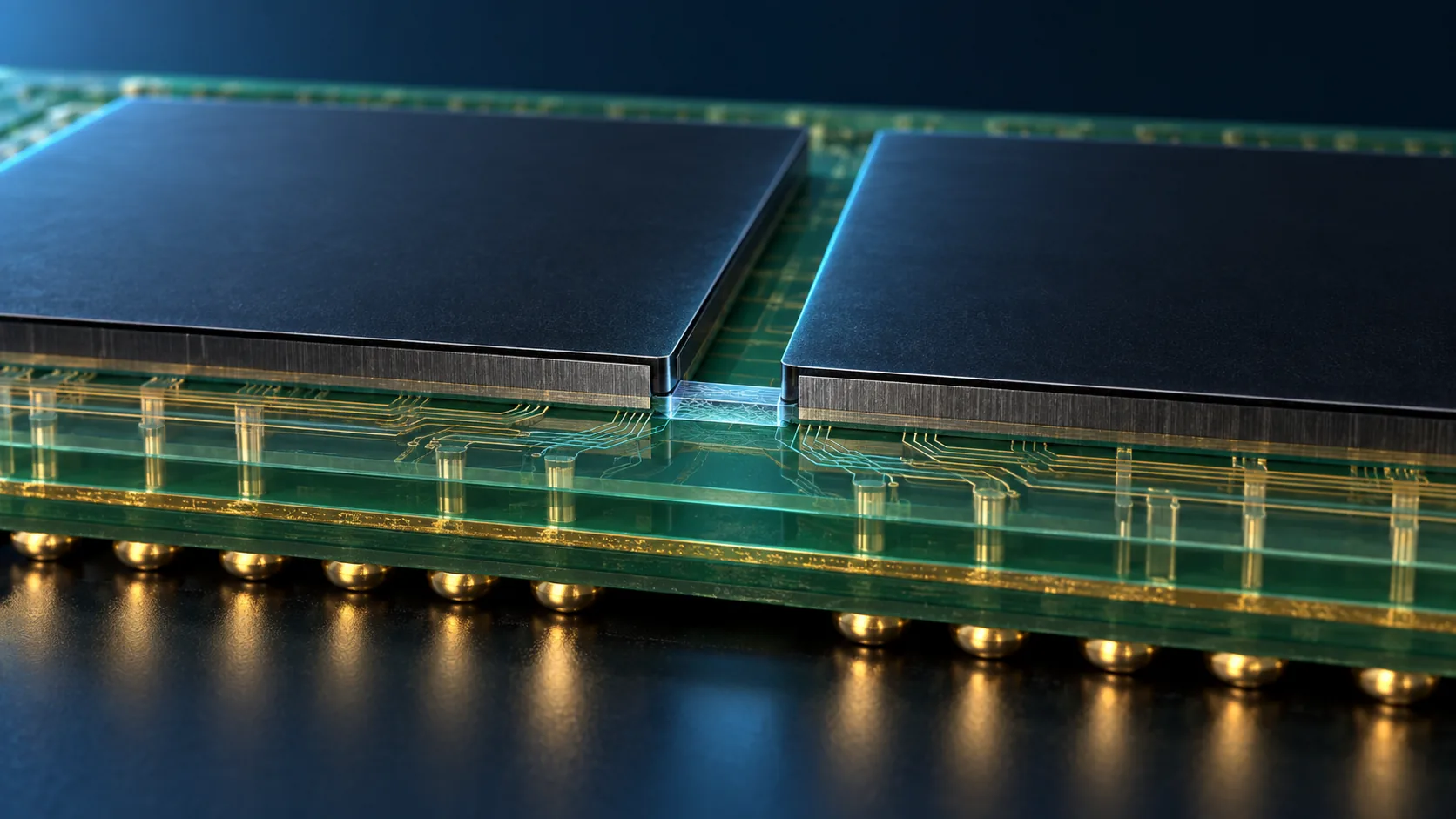
Linking chips to each other at fine pitch takes silicon wiring. But make the whole package out of silicon and it turns expensive, stiff and impossible to grow. So you bury one small piece of silicon exactly where the link has to happen — that is a bridge. Seen from the materials side, the question becomes how far to lean on silicon at all.
- What a bridge is (the short version)
- Why a full sheet of silicon is not the answer
- EMIB — burying silicon inside the substrate
- A materials engineer's view 1: two bump pitches on one die
- A materials engineer's view 2: the bridge stops being wiring and becomes a component
- Bridges from each supplier
- What is still hard
- Glossary / Primary sources / Claim-to-source audit
Sourced = a value stated in published material from a research institute or manufacturer (link given)
Our calculation = a figure this article derived, with the assumptions spelled out
Not yet confirmed = research-stage work with no confirmed production record
Beyond those, any structural reading or materials-design interpretation is set apart as Commentary.
1. What a bridge is (the short version)
A bridge is a small piece of silicon embedded in the package substrate for one purpose only: to link two neighbouring chips.
- What it does: carries fine silicon wiring across the gap between the facing edges of two dies
- What it does not do: it does not sit under the whole die. Power and every other signal go through the substrate
- Why bother: silicon gives the finest wiring of any option, but it is expensive, stiff, and cannot be made large
Intel describes EMIB (Embedded Multi-die Interconnect Bridge) as "the industry's first 2.5D interconnect solution using bridges embedded in the substrate", and states that it has been "In high-volume manufacturing since 2017"Sourced.
Bridges have already appeared in several other articles. This one tackles them head on.
- A full sheet of silicon as the interposer → the Interposer article and the CoWoS article (CoWoS-S)
- An organic RDL interposer → the RDL article and the CoWoS article (CoWoS-R)
- Bridges → this article (EMIB, CoWoS-L, S-Connect)
2. Why a full sheet of silicon is not the answer
The most straightforward way to link chips at high density is to lay down a large silicon plate and put everything on top of it. That is the silicon interposer, and TSMC's CoWoS-S is exactly this.
Intel puts the difference like this: "EMIB uses a very small bridge die with multiple routing layers, instead of the large silicon interposer typically used in other approaches"Sourced.
Intel is specific about what that buys you: "The small footprint of EMIB means that the balance of the input/output (I/O) signal and the power-integrity characteristics are unaffected. This contrasts with a full silicon interposer, which requires all signal and power vias to traverse through the interposer."Sourced.
3. EMIB — burying silicon inside the substrate
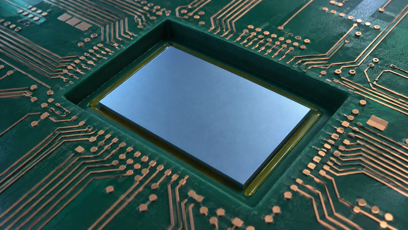
So how does it get buried? Intel's account is short: "EMIB places bridges in the substrate cavity where they are held in place with adhesives. The process adds dielectric and metal build-up layers."Sourced.
And then comes the sentence that matters most: "The EMIB process uses standard semiconductor package-assembly flows, with the only difference being the manufacturing of the substrate."Sourced.
That sentence is also a statement about how the industry is organised. If the only difference is the manufacturing of the substrate, then the assembly house can keep running its ordinary flip-chip flowSourced.
In exchange, the substrate maker takes on a new job: cut a cavity, place a piece of silicon in it accurately with adhesive, and build up layers on top of it.
The lamination and fine-line wiring covered in the Package Substrate and Build-up Film articles are being stretched into a new skill: burying a foreign object and still building up flat on top of it — which is the same territory as glass cores and panel-level packaging (Commentary).
On assembly yield Intel states: "They achieve assembly yields comparable to a standard flip chip ball grid array (FCBGA) of equal complexity."Sourced.
4. A materials engineer's view 1: two bump pitches on one die
This is the cleverest part of the whole scheme. Intel writes:
"Combining two different bump pitches on the die enables cost-efficient heterogeneous integration and scaling for very large complexes. EMIB requires a tight microbump pitch at the bridge only, which allows the rest of the die-core region to retain a loose pitch"Sourced.
As the Bumps article showed, the tighter the pitch, the harder both the joining and the filling become. The intermetallic fraction rises, and underfill filler stops fitting through the gap.
With EMIB, that difficulty is confined to the narrow strip running over the bridge rather than the whole die faceSourced. The remaining area can keep the coarse bumps it always had.
In terms of what the materials must deliver, that split matters:
- The fine strip: underfill with small-diameter filler, and precise joining
- The coarse remainder: conventional materials and conventional processes are enough
Two zones with very different requirements now live under a single die. And only one underfill gets poured in. The material has to be specified for the worst spot and then used everywhere — the split between CUF for Top and CUF for Bottom seen in the Underfill article reappears here inside one die (Commentary).
5. A materials engineer's view 2: the bridge stops being wiring and becomes a component
A bridge started life as nothing more than a wiring plate. Suppliers are now loading functions onto it.
Intel describes EMIB-M as a version that "incorporates Metal Insulator Metal (MIM) capacitors into the silicon bridges to enhance power delivery", and for EMIB-T writes that "The demand for high-bandwidth memory (HBM) has increased the need for vertical power delivery with minimal DC and AC noise. To respond to this, Intel Foundry has added through-silicon vias (TSVs) to the EMIB-T solution."Sourced.
Amkor is heading the same way. For S-Connect it says the technology offers improved power delivery network (PDN) and signal integrity through embedded IPD, and uses molded Cu tall pillars for vertical pass-through signal and power deliverySourced.
What EMIB-M, EMIB-T and S-Connect have in common is that the bridge has been given work beyond simply linking diesSourced.
- Capacitors: sitting right next to the load, they damp the voltage swing
- TSVs and Cu tall pillars: make the bridge conductive vertically too, so power can come up from below
The striking part is that the TSV has come back. One of the selling points of a bridge was that it needed no TSVs at all, yet the demand for vertical power delivery has pushed the design towards opening TSVs only where they are neededSourced.
From doing everything to doing only what is needed. The idea behind the bridge is, in other words, being applied a second time inside the bridge itself (Commentary).
6. Bridges from each supplier
| Technology | Supplier | What the published material says |
|---|---|---|
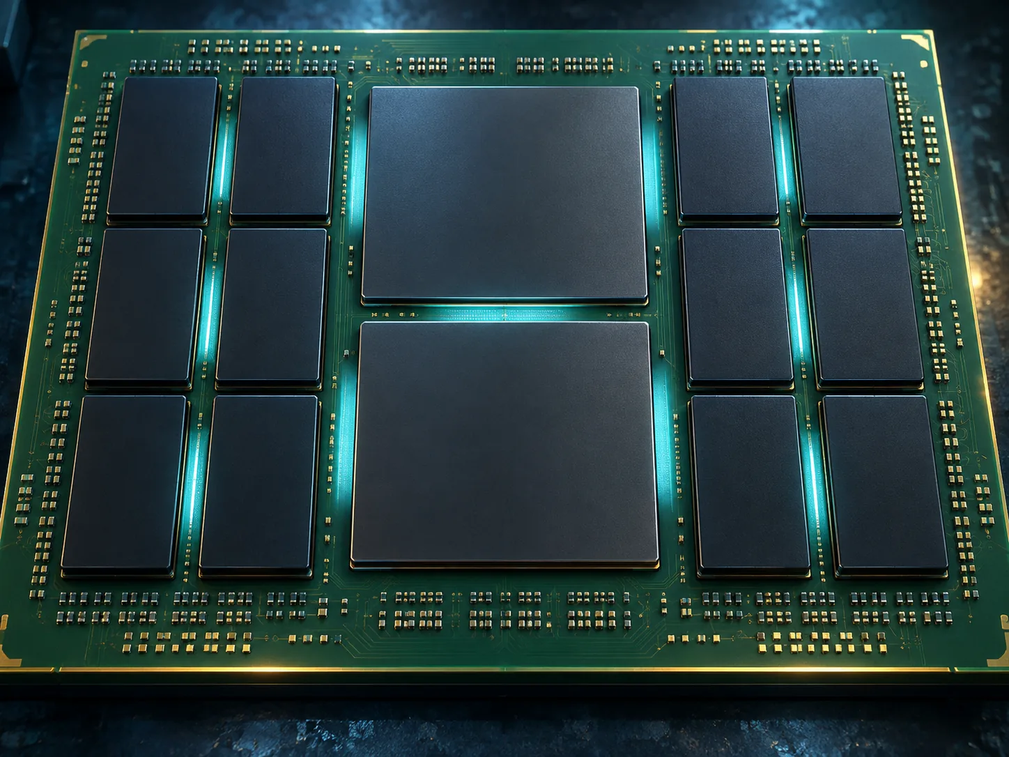
| EMIB | Intel | "The industry's first 2.5D interconnect solution using bridges embedded in the substrate", in high-volume manufacturing since 2017. Bridges are placed in a substrate cavity, held with adhesives, and dielectric and metal build-up layers are added on top |
| EMIB-M | Intel | MIM capacitors are incorporated into the silicon bridges to enhance power delivery |
| EMIB-T | Intel | TSVs added to meet the demand for vertical power delivery with minimal DC and AC noise for HBM |
| EMIB 3.5D | Intel | A hybrid configuration combining EMIB with Foveros (2.5D and Direct 3D) in a single package |
| CoWoS-L | TSMC | Combines an RDL-based interposer with higher-density embedded local silicon interconnect (LSI), eDTC and integration of various embedded chips |
| S-Connect | Amkor | An embedded silicon bridge die for die-to-die connection. Embedded IPD improves power delivery and signal integrity. Molded Cu tall pillars carry vertical signal and power. An extension of the proven HDFO technology (S-SWIFT) |
| i-THOP (in development) | Shinko Electric | A "substrate for 2.3D packages" that integrates an organic interposer with a build-up substrate, positioned as a replacement for 2.5D packages |
All entries come from the suppliers' own published material [Sources 1, 2, 3, 5 and 6]. i-THOP is explicitly labelled as being in development, and we have not confirmed any production record. CoWoS-L combines an RDL interposer with bridges, so its construction differs from EMIB, which buries the bridge in the substrate.
The industry is moving too. On 30 April 2025 Amkor announced that "Amkor Technology has entered into a Strategic Partnership with Intel focused on Embedded Multi-Die Interconnect Bridge (EMIB) assembly.", saying the work would be supported at its facilities in Korea, Portugal and ArizonaSourced. That is the same shifting boundary between foundry and contract assembly described in the OSAT article, showing up again here.
7. What is still hard
(1) Less silicon, but never zero
Here is a rough estimate, on assumed dimensions, of how much silicon area the bridge approach savesOur calculation.
- Assumption: the interposer-equivalent area of the package is 55 × 55 mm (= 3,025 mm²)
- Assumption: eight bridges link the compute dies to the HBM stacks, each 3 × 12 mm (= 36 mm²)
- Total bridge area = 36 × 8 = 288 mm²
- Fraction of the full area = 288 ÷ 3,025 ≈ 9.5 %
Every assumption here was set by this article and none of them is a dimension of any real product. Even so the conclusion is clear: the silicon area can be made an order of magnitude smaller. But it never reaches zero. Wherever dies are linked, silicon is still required — and that is precisely where the bridge approach sits (Commentary).
(2) Once buried, it cannot be taken back out
The bridge is fixed inside the substrate with adhesive, and build-up layers are stacked on top of itSourced. In other words, by the time the substrate is finished the bridge is sealed inside it. One faulty bridge makes the whole substrate unusable. The known good die (KGD) problem discussed in the Test and Co-Packaged Optics articles reappears here as a problem for the substrate maker (Commentary).
(3) The step, and staying flat
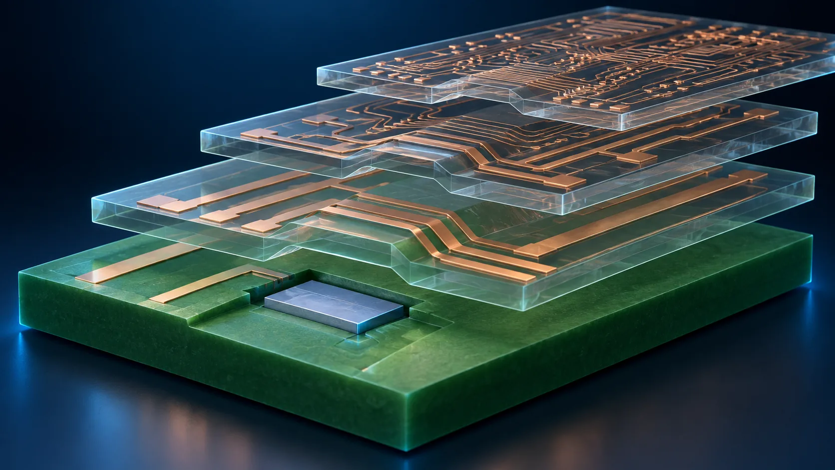
Drop a piece of silicon into a cavity and you inevitably leave a small step. The build-up layers and the fine wiring stacked above it have to climb over that step. The depth of focus of the CO₂ laser discussed in the Via article, and the thickness variation discussed in the Build-up Film article, both get harder once a foreign object is buried in the substrate (Commentary).
The bridge is the clearest example in back-end packaging of a single idea: use less of the expensive thing.
- Less silicon: only the strip that carries the link, not the whole area
- Less fine pitch: only directly above the bridge, not the whole die face
- Fewer TSVs: only where power has to rise, not right across the plate (EMIB-T, Cu tall pillars)
What was saved, though, has moved to the substrate side as a different kind of difficulty. Cut the cavity, place the piece accurately, bond it, then wire across the step. A silicon problem has been turned into a substrate problem — that is what the bridge approach looks like from the materials side (Commentary).
8. Glossary
- Bridge
- A small piece of silicon embedded in the substrate to link neighbouring chips.
- EMIB
- Embedded Multi-die Interconnect Bridge. Intel's bridge technology, in production since 2017.
- EMIB-M
- A bridge with MIM capacitors built in to strengthen power delivery.
- EMIB-T
- A bridge with TSVs added so that power can be delivered vertically.
- EMIB 3.5D
- A configuration combining EMIB and Foveros (stacking) in a single package.
- LSI (CoWoS-L)
- Local Silicon Interconnect. The embedded silicon interconnect TSMC uses in CoWoS-L.
- S-Connect
- Amkor's embedded silicon bridge technology, combined with IPD and Cu tall pillars.
- MIM capacitor
- Metal Insulator Metal. A capacitor formed from a metal / dielectric / metal sandwich.
- IPD
- Integrated Passive Device. Resistors and capacitors integrated into one passive component.
- TSV
- Through Silicon Via. An electrode that passes through silicon (covered in the TSV article).
- Cu tall pillar
- A tall copper post set in resin, used as a vertical signal or power path.
- HDFO
- High Density Fan-Out. A high-density fan-out package.
- Build-up layer
- A structure made by stacking dielectric and wiring layers one at a time on a substrate (covered in the Package Substrate article).
- Cavity
- The recess cut into the substrate that holds the bridge.
- FCBGA
- Flip Chip Ball Grid Array. A BGA package assembled flip-chip.
- 2.3D
- The term Shinko Electric uses for its substrate with an integrated organic interposer.
9. Primary sources
- Intel "Embedded Multi-die Interconnect Bridge (EMIB) revolutionizes chip packaging interconnect technology", Technology Brief, July 2025 (PDF) — intel.com
- Intel Foundry "Advanced Packaging Innovations" — intel.com
- Amkor "S-Connect™" — amkor.com
- Amkor "Amkor-Intel Partnership Expands US EMIB Packaging Capacity", 30 April 2025 — amkor.com
- TSMC "CoWoS®" technology page — 3dfabric.tsmc.com
- Shinko Electric "Substrate for 2.3D packages: i-THOP® (in development)" (Japanese-language page) — shinko.co.jp
10. Claim-to-source audit
| Claim in the text | Basis | Label |
|---|---|---|
| That EMIB is "the industry's first 2.5D interconnect solution using bridges embedded in the substrate" and "In high-volume manufacturing since 2017". "EMIB uses a very small bridge die with multiple routing layers, instead of the large silicon interposer typically used in other approaches". "EMIB places bridges in the substrate cavity where they are held in place with adhesives. The process adds dielectric and metal build-up layers." "The EMIB process uses standard semiconductor package-assembly flows, with the only difference being the manufacturing of the substrate." "The small footprint of EMIB means that the balance of the input/output (I/O) signal and the power-integrity characteristics are unaffected. This contrasts with a full silicon interposer, which requires all signal and power vias to traverse through the interposer." "Combining two different bump pitches on the die enables cost-efficient heterogeneous integration...EMIB requires a tight microbump pitch at the bridge only, which allows the rest of the die-core region to retain a loose pitch". "They achieve assembly yields comparable to a standard flip chip ball grid array (FCBGA) of equal complexity." That EMIB-M incorporates MIM capacitors, that EMIB-T adds TSVs for vertical power delivery for HBM, and that EMIB 3.5D is a hybrid of EMIB and Foveros | Intel "EMIB Technology Brief", July 2025[Source 1] https://www.intel.com/content/dam/www/central-libraries/us/en/documents/2025-07/emib-product-brief.pdf | Sourced |
| That EMIB 2.5D is a "Silicon bridge embedded in package substrate" and "Production proven: In mass production since 2017 with Intel and external silicon". That Foveros-S is a "Silicon interposer with 4x reticle" in production since 2019. That Foveros Direct uses a "Cu-to-Cu hybrid bonding interface (HBI)" | Intel Foundry "Advanced Packaging Innovations"[Source 2] https://www.intel.com/content/www/us/en/foundry/packaging.html | Sourced |
| That S-Connect delivers high-bandwidth device-to-device interconnect through an embedded silicon bridge die for die-to-die connection; that embedded IPD improves power delivery network (PDN) and signal integrity; that molded Cu tall pillars are used for vertical pass-through signal and power delivery; and that it is an extension of the proven HDFO technology (S-SWIFT) | Amkor "S-Connect™"[Source 3] https://amkor.com/technology/s-connect/ | Sourced |
| That on 30 April 2025 Amkor announced "Amkor Technology has entered into a Strategic Partnership with Intel focused on Embedded Multi-Die Interconnect Bridge (EMIB) assembly." and that the work is supported in Korea, Portugal and Arizona | Amkor blog, 30 April 2025[Source 4] https://amkor.com/blog/amkor-intel-partnership-expands-us-emib-packaging-capacity/ | Sourced |
| That CoWoS-L combines an RDL-based interposer with higher-density embedded local silicon interconnect (LSI), eDTC and the integration of various embedded chips | TSMC "CoWoS®" technology page[Source 5] https://3dfabric.tsmc.com/english/dedicatedFoundry/technology/cowos.htm | Sourced |
| That i-THOP is a "substrate for 2.3D packages" integrating an organic interposer with a build-up substrate, positioned as a replacement for 2.5D packages, and that its stated applications are splitting a logic chip, mixing a logic chip with high-bandwidth memory, mounting HBM-class memory and integrating chiplets | Shinko Electric "i-THOP®" (Japanese-language page)[Source 6] https://www.shinko.co.jp/product/package/substrate/i-thop.php | Sourced |
| That the page labels i-THOP as being in development, and that no production record has been confirmed | Shinko Electric "i-THOP®" (Japanese-language page)[Source 6] https://www.shinko.co.jp/product/package/substrate/i-thop.php | Not yet confirmed |
| Fig. 7: an area ratio of about 9.5 %, assuming an interposer-equivalent region of 55 × 55 mm (3,025 mm²) and eight bridges of 3 × 12 mm (36 mm² each, 288 mm² in total) | Our calculation. Every dimension is an assumption set by this article and none is a value for a real product. Real bridge sizes and counts differ from product to product | Our calculation |
| The reading that the difficulty was pushed onto the substrate maker. The observation that only the fine-pitch zone raises the demands on the underfill while just one resin is dispensed. The reading that the TSV has returned, only where it is needed. The observation that a buried bridge turns the KGD question into the substrate maker's problem. The observation that placing silicon in a cavity leaves a step that affects build-up and fine wiring. The summary that a silicon problem has been turned into a substrate problem. Drawing the two routes as arrows in Fig. 2 | Commentary: this article's own structuring and reading of published material. Not a position stated by any of the companies | Commentary |
| That the cross-sections and plan views in Figs. 1, 2, 4 and 5 are explanatory drawings rather than real micrographs or design data | A note by this article | Commentary |
Last updated 20 September 2026. Sources are limited to primary material (official technical documents and product pages from semiconductor, packaging and substrate manufacturers). Because the text also contains structural readings and materials-design interpretation, those are set apart as Commentary and kept separate from sourced fact. All figures are explanatory concept graphics. Visual-overview figures are shown as AI-generated conceptual images, matching the Japanese edition. Vector drawings are retained where they carry quantitative values or precision-critical technical labels. AI-generated images do not depict real equipment, products, facilities, dimensions or exact cross-sections; replaced source SVG overview drawings remain in the HTML but are hidden.