TECHNOLOGY EXPLAINER
What Buildup Film Is
— how ten micrometres of plastic decide what an AI chip can do
Buildup film is the insulating material that the wiring layers of a semiconductor package substrate are built on. It looks like one of the least glamorous parts in the package. Read its datasheet, though, and you can watch three demands — faster signals, finer lines, flatter boards — pull against one another in plain numbers.
- What buildup film is (the short version)
- Why a film, and not a liquid
- Where it sits in the process
- Reading the performance demands off real data
- A materials engineer's view: the trade-offs the numbers admit to
- Rough or smooth: a dilemma with no free answer
- Who supplies it — ABF, and the newcomers
- What is still hard
- Glossary / Primary sources / Claim-to-source audit
Sourced = a value stated in published material from a research institute or manufacturer (link given)
Our calculation = a figure this article derived, with the assumptions spelled out
Not yet confirmed = research-stage work with no confirmed production record
Beyond those, passages that read the published numbers or describe a general materials mechanism are marked Commentary.
1. What buildup film is (the short version)
Sekisui Chemical describes the material this waySourced.
"Buildup film is the interlayer insulating material used to form the fine wiring layers of leading-edge IC package substrates" (Sekisui Chemical, Japanese-language page)
- Where it goes: it is the insulating part of the buildup layers stacked above and below the core of a package substrate
- What form it takes: a film, not a liquid. You laminate it, then cure it
- What it is for: it keeps copper traces apart, and at the same time provides the ground those traces are grown on
It is thin. Ajinomoto puts ABF (Ajinomoto Build-up Film) at roughly 10 µm per layerSourced. Sekisui offers its own range in thicknesses from 20 to 100 µm, in 2.5 µm stepsSourced.
The Package Substrate article covered buildup layers and ABF as parts of a structure. This one puts the insulating material itself in the lead role and reads it through its physical properties. Same material, approached from the materials side rather than the structural side.
2. Why a film, and not a liquid
It feels obvious now, but this material started life as a liquid ink. Ajinomoto explains why it moved to film formSourced.
The older liquid inks were prone to uneven coating, trapped air bubbles and harmful outgassing. They also had to be coated and dried one face at a time, twice over, which was inefficient. Switching to a film meant both faces could be processed in a single lamination, cutting four steps down to one (Ajinomoto, Japanese-language page).
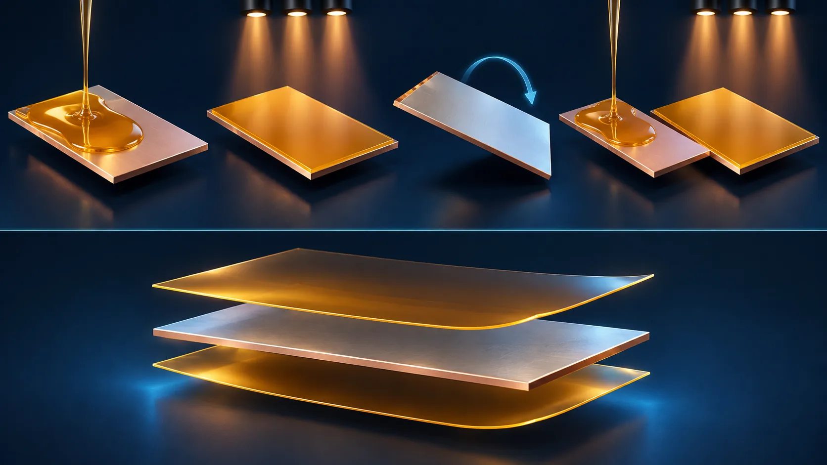
Without changing the chemistry at all, simply shipping the same resin as a film instead of a liquid cut the customer's process to a quarter. A materials supplier's value lies not only in what the product is made of but in the form it arrives in. Few examples make that as plainly as this one.
Section 5 shows another case where the form of supply — liquid against granulate — reaches through to thermal properties and changes the manufacturing outcome. Form is part of performance.
3. Where it sits in the process
Laminating the film is not the end of the story. The material itself is then machined, etched and plated on.
- Lamination: pressed onto the core, or onto the wiring layer below it, under vacuum
- Cure: heated so the resin cross-links
- Laser drilling: microvias are opened through it to reach the layer below
- Desmear and roughening: resin residue inside the hole is stripped away, and the surface is roughened in the same step
- Electroless then electrolytic plating (SAP): copper is grown on the roughened surface to form the wiring
Sekisui states that its buildup film suits the semi-additive process (SAP) and runs stably across a wide process window, and that it has a production record at several substrate makers in Japan and Taiwan and at major OSATsSourced.
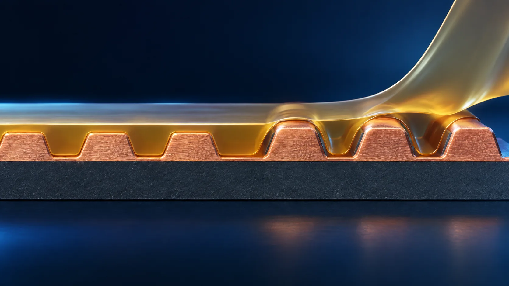
Sekisui lists "good embedding" among its product's strengthsSourced. The surface the film is laminated onto is not flat: there are copper traces underneath, with valleys between them. If the resin does not flow into those valleys completely, voids are left behind. Yet the film also has to stay thin and even. It must flow, but not flow too much — designing that flow behaviour at lamination temperature is the hard part of a laminating material.
4. Reading the performance demands off real data
Sekisui Chemical publishes the properties of four of its buildup film productsSourced. A whole product family from one maker, laid out side by side, is rare and useful data.
| Property | NX04H (in production) | NQ07V (sample) | QX04 (sample) | EL |
|---|---|---|---|---|
| Dissipation factor Df @10GHz | 0.0079 | 0.0038 | 0.0024 | ≤0.0025 |
| Dielectric constant Dk @10GHz | 3.4 | 3.5 | 3.3 | ≤2.5 |
| CTE (25 to 150 °C) | 24.5 ppm/°C | 27 ppm/°C | 15 ppm/°C | 17 to 23 ppm/°C |
| Glass transition temperature Tg (DMA) | 205 °C | 183 °C | 177 °C | — |
| Young's modulus | 8.0 GPa | 10.4 GPa | 14.0 GPa | — |
| Elongation at break | 2.4% | 2.6% | 2.9% | — |
| Tensile strength | 100 MPa | 105 MPa | 110 MPa | — |
| Thermal conductivity | 0.46 W/m·K | 0.46 W/m·K | 0.62 W/m·K | — |
All Sourced (Sekisui Chemical, Japanese-language page). Dk and Df are split-cylinder values at 10 GHz. NX04H is in high-volume manufacturing; NQ07V and QX04 are described as sample grades.
5. A materials engineer's view: the trade-offs the numbers admit to
Read that table asking which product is best and you learn nothing. Follow the differences between the products and the design intent comes into view.
1. Low loss and heat resistance move in opposite directions
Df improves from 0.0079 to 0.0038 to 0.0024, a factor of more than three,
while Tg goes 205 °C, 183 °C, 177 °C — 28 °C lower.
Lowering dielectric loss means suppressing molecular polarity and opening up free volume,
and that direction generally costs you heat resistance.
A textbook trade-off, showing up unretouched in a commercial product family.
2. Low expansion and stiffness travel together
QX04 has a strikingly low CTE of 15 ppm/°C, and the highest Young's modulus of the three at 14.0 GPa.
More inorganic filler accounts for the pair of them: add filler and CTE falls while stiffness rises.
Thermal conductivity rises too, 0.46 to 0.62 W/m·K, which fits the same explanation.
3. And yet the elongation did not suffer
More filler normally makes a resin brittle, but elongation at break goes up, 2.4% to 2.9%.
Tensile strength rises as well, 100 to 110 MPa. This is where formulation skill shows.
Highly filled, low-CTE and stiff, without turning brittle —
that is presumably the context in which Sekisui lists "high crack resistance" as a strengthSourced.
6. Rough or smooth: a dilemma with no free answer
Buildup film has one more hard problem that never appears on a datasheet: surface roughness.
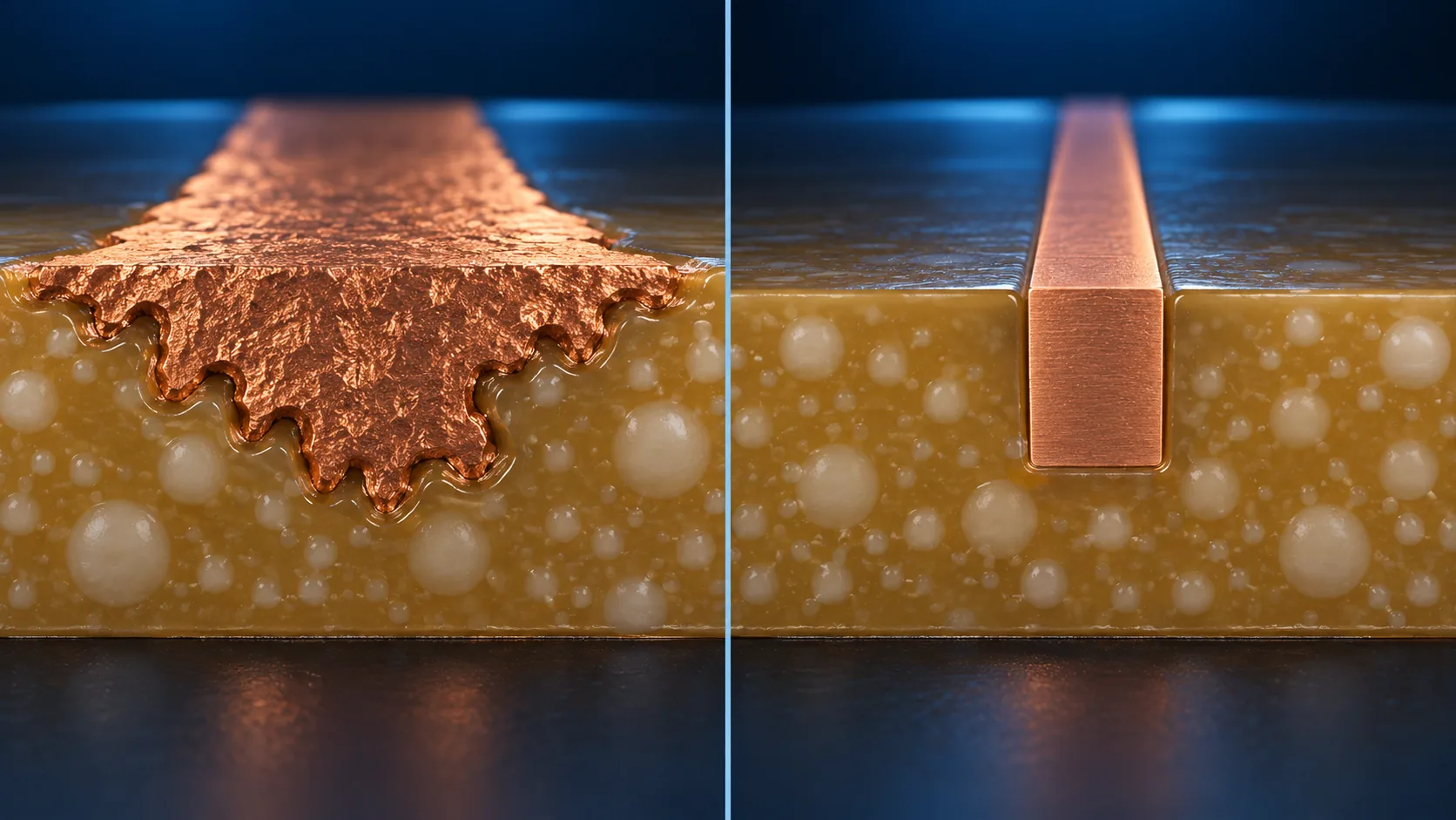
Taiyo Holdings describes its thermosetting buildup film as "a thermosetting insulating film for the semi-additive process, with high peel strength even when the surface after roughening is left at low roughness", and lists high Tg, a smooth surface and stable peel strength for plated copper as features of its epoxy-based productSourced (Taiyo Holdings, Japanese-language page).
Sekisui gives its own strengths as "low dissipation factor, uniform surface roughness after desmear, and high crack resistance"Sourced.
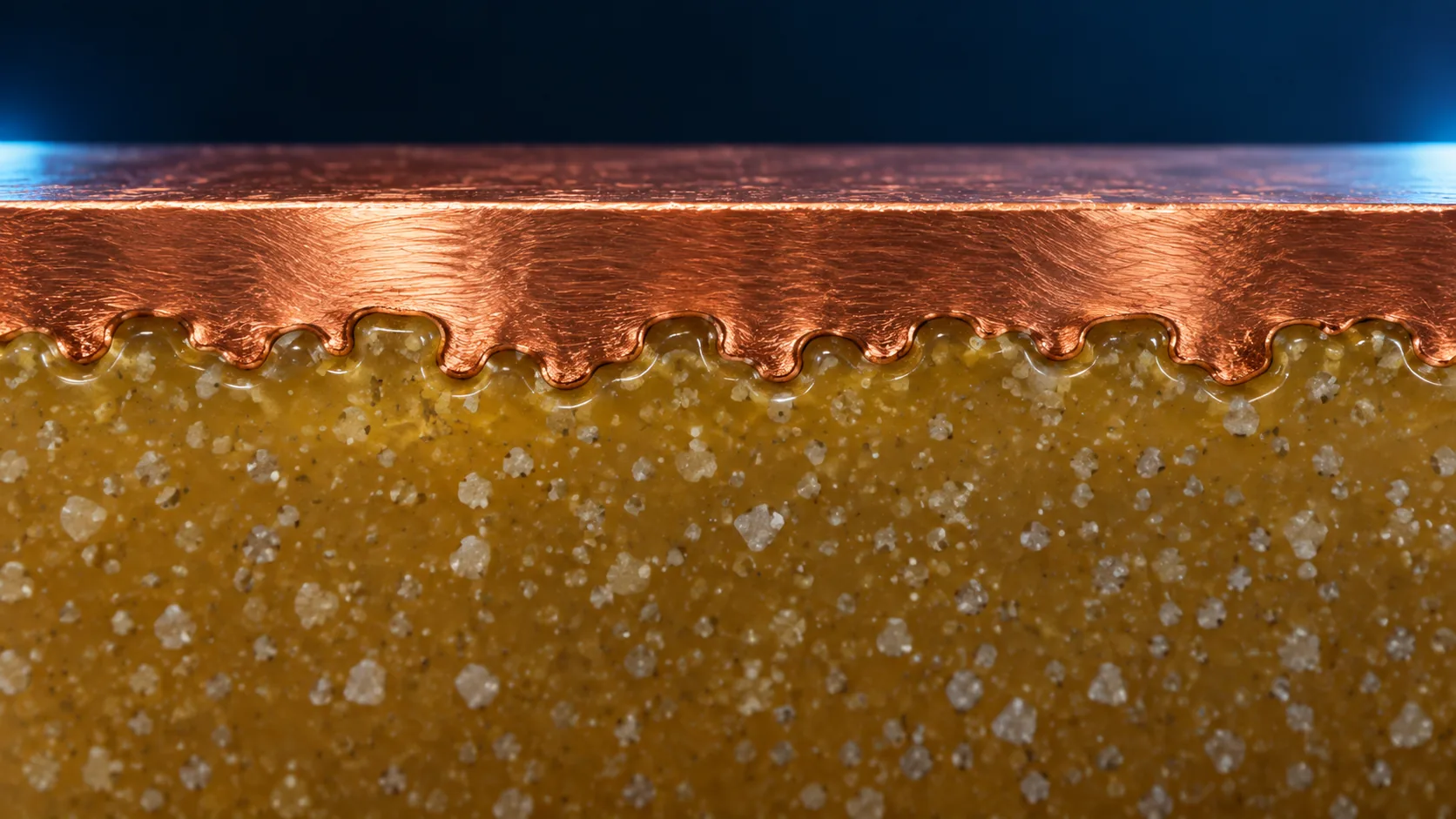
Roughness is not something you simply want less of, nor more of. What matters is that it does not vary across the panel.
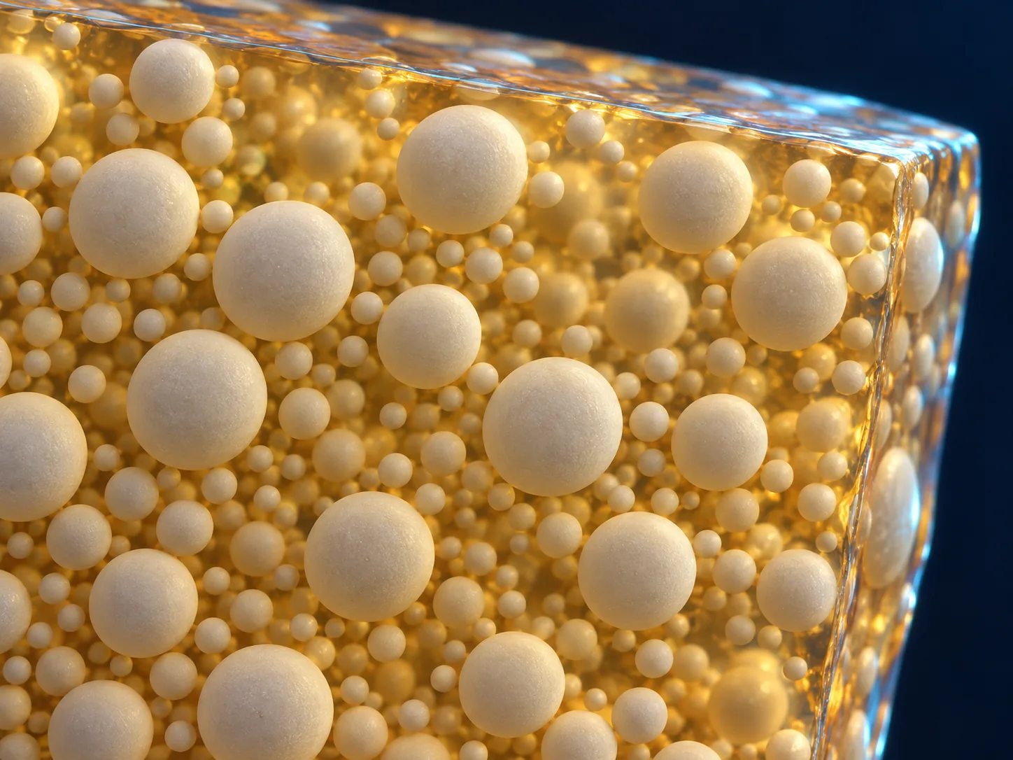
Desmear is a wet chemical step, so wherever the resin's composition or state of cure differs, the rate of attack differs too. If roughness varies, copper lifts in one place while lines fail to resolve in another. You have to engineer the distribution, not the mean — which is the territory of filler particle size distribution and state of dispersion.
7. Who supplies it — ABF, and the newcomers
For a long time this material had one name: ABF, Ajinomoto Build-up Film. Ajinomoto says it was adopted by a major semiconductor maker in 1999 and is now used in close to 100% of mainstream personal computersSourced (Ajinomoto, Japanese-language page. Another of the company's pages gives the figure as about 95%).
Investing in capacity
On 7 May 2026, Ajinomoto and Ajinomoto Fine-Techno announced that they had acquired land for a new plant in the Kani-Mitake Interchange Industrial Park in Kani City, Gifu PrefectureSourced.
| Item | As announced |
|---|---|
| Location | Kani-Mitake Interchange Industrial Park, Kani City, Gifu Prefecture |
| Acquisition cost | About 1.2 billion yen |
| Purpose of the site | A production base for ABF, the interlayer insulating material for semiconductor packages |
| Rationale | Expanding capacity, and strengthening supply stability from a business-continuity standpoint |
| Demand outlook | Strong growth expected to continue, driven by cloud services, AI data centres and networking |
| Timing | Construction from 2028, operation from 2032 |
All Sourced (Ajinomoto, 7 May 2026, Japanese-language release).
Land acquired now, production in 2032. Capacity in semiconductor materials does not appear on demand. However sharply AI demand rises, a materials plant answers on a timescale of years — a sense of pace worth keeping in mind whenever supply constraints come up.
Who else is in the field
Meanwhile this is no longer a one-company business. Several Japanese suppliers are in it, each entering from a different angle.
| Company | What they have published |
|---|---|
| Ajinomoto | ABF. Adopted in 1999, close to 100% of mainstream PCs. Land acquired in Kani City for a new plant (construction from 2028, operation from 2032) |
| Sekisui Chemical | Thermosetting interlayer insulating film. Strengths given as low Df, uniform roughness after desmear, high crack resistance. Thicknesses 20 to 100 µm in 2.5 µm steps. TOPPAN and Nan Ya PCB named as customers. Production record at substrate makers in Japan and Taiwan and at major OSATs |
| Taiyo Holdings | Thermosetting buildup film, Zaristo 125G. High peel strength even at low roughness, SAP compatible, epoxy based, high Tg |
| Resonac | Photosensitive interlayer insulating film (PV-F). Aimed at embedded-component substrates, supporting large cavity formation and large numbers of thermal vias |
All Sourced (each company's published pages). The products target different applications, so they are not necessarily in direct competition.
8. What is still hard
(1) Pushing Df lower still
Across Sekisui's family, Df falls from 0.0079 in the production grade to 0.0024 in a sample gradeSourced. There is room left to go lower, but each step is paid for in Tg or some other property — exactly as Section 5 showed.
(2) Bigger substrates, more layers
Sekisui positions the material as "an insulating material that delivers both lower transmission loss and warpage control in high-layer-count, large-format IC package substrates"Sourced. The larger the format, the harder warpage becomes to hold.
(3) A different foundation underneath
As the Glass Substrate article described, there is a move to replace the core layer with glass. Buildup layers are what gets stacked above and below that core, so a change of foundation changes what is asked of them Not yet confirmed. The shift to rectangular panels covered in the PLP article adds another new condition: thickness uniformity over a large area.
(4) Photosensitivity as an alternative
Instead of drilling holes with a laser, the material can be made photosensitive and the holes opened by exposure and development — the approach covered in the RDL article. That Resonac has commercialised a photosensitive interlayer insulating film shows the boundary between buildup film and RDL materials closing upSourced.
9. Glossary
- Buildup film
- The film-form interlayer insulating material used in the buildup layers of a package substrate.
- ABF
- Ajinomoto Build-up Film. For years the name that stood for the whole category.
- Interlayer insulating material
- The material that electrically separates one wiring layer from the next.
- Lamination
- The step that presses the film down, under vacuum, so it follows the topography below.
- Desmear
- Wet chemical removal of resin residue left after laser drilling. It roughens the surface at the same time.
- SAP
- Semi-additive process. Fine wiring formed by growing copper only where it is wanted.
- Peel strength
- The force needed to pull plated copper off the resin. The usual measure of adhesion.
- Df (dissipation factor)
- The fraction of signal energy turned into heat. Lower is better for fast signals.
- Dk (dielectric constant)
- The material's permittivity. Lower means signals travel faster.
- CTE
- Coefficient of thermal expansion. Lower helps against warpage.
- Tg
- Glass transition temperature. Above it the resin softens; higher means better heat resistance.
- Young's modulus
- Stiffness. Higher resists deformation but gives stress fewer places to go.
- Inorganic filler
- Fine particles mixed into the resin. They lower CTE and raise stiffness and thermal conductivity.
- Embedding
- How completely the resin fills the gaps in the wiring topography beneath it.
- Split-cylinder method
- One of the standard ways of measuring dielectric properties at high frequency.
10. Primary sources
- Sekisui Chemical "Thermosetting interlayer insulating film" product page (Japanese-language page) — sekisui.co.jp
- Ajinomoto "ABF" innovation story (Japanese-language page) — ajinomoto.co.jp
- Ajinomoto "What is ABF, the insulating film born out of AminoScience®?" (Japanese-language page) — story.ajinomoto.co.jp
- Ajinomoto "Ajinomoto Co. and Ajinomoto Fine-Techno acquire land for a new plant", 7 May 2026 (Japanese-language release) — news.ajinomoto.co.jp
- Taiyo Holdings "Thermosetting buildup film" product page (Japanese-language page) — taiyo-hd.co.jp
- Resonac "Free your thermal design for power-device embedded substrates: photosensitive interlayer insulating film" (Japanese-language page) — resonac.com
- Resonac "Materials that help control warpage and relieve stress in advanced semiconductor packages, part 2", 20 May 2026 (Japanese-language page) — resonac.com
11. Claim-to-source audit
| Claim in the text | Basis | Label |
|---|---|---|
| The definition of buildup film; that fine via formation, low dielectric loss and dimensional stability matter; that it is positioned as a material delivering both lower transmission loss and warpage control in high-layer-count, large-format substrates | Sekisui Chemical product page[Source 1] https://www.sekisui.co.jp/electronics/ja/semicon/Insulationfilm.html | Sourced |
| Properties of the four Sekisui products (Df and Dk at 10 GHz by split cylinder, CTE 25 to 150 °C, Tg by DMA, Young's modulus, elongation, tensile strength, thermal conductivity); thicknesses 20 to 100 µm in 2.5 µm steps; strengths given as low Df, uniform roughness after desmear and high crack resistance; TOPPAN and Nan Ya PCB as customers; production record in Japan and Taiwan; SAP compatibility; "good embedding" | Sekisui Chemical product page[Source 1] https://www.sekisui.co.jp/electronics/ja/semicon/Insulationfilm.html | Sourced |
| The reading that Tg falls as Df improves, that Young's modulus rises as CTE falls, and that elongation and strength do not suffer | The result of this article plotting and comparing the published values above. No causal claim of this kind is made by the manufacturer | Commentary |
| That liquid inks suffered uneven coating, bubbles and harmful outgassing and had to be coated twice, one face at a time; that moving to film cut four steps to one | Ajinomoto story page[Source 3] https://story.ajinomoto.co.jp/rd/017.html | Sourced |
| That ABF was adopted in 1999 and is used in close to 100% of mainstream PCs (about 95% on another page), at roughly 10 µm per layer | Two Ajinomoto published pages[Source 2] https://www.ajinomoto.co.jp/company/jp/rd/our_innovation/abf/[Source 3] https://story.ajinomoto.co.jp/rd/017.html | Sourced |
| Land acquired in Kani City, about 1.2 billion yen, construction from 2028 and operation from 2032, supply stability including business continuity, high growth expected on the back of AI data centre and related demand | Ajinomoto news release, 7 May 2026[Source 4] https://news.ajinomoto.co.jp/2026/05/20260507-02.html | Sourced |
| Taiyo Holdings Zaristo 125G: high peel strength even at low roughness after roughening, SAP compatible, epoxy based, high Tg, smooth surface, stable peel strength for plated copper | Taiyo Holdings product page[Source 5] https://www.taiyo-hd.co.jp/jp/products/thermal-curable-build-up-film/ | Sourced |
| That Resonac has commercialised a photosensitive interlayer insulating film (PV-F) supporting large cavity formation and many thermal vias | Resonac product page[Source 6] https://www.resonac.com/jp/solution/PV-F.html | Sourced |
| The roughness-versus-smoothness trade-off; that uniformity of roughness relates to filler particle size distribution and dispersion; that more filler is consistent with lower CTE, higher stiffness and higher thermal conductivity | Commentary based on general relationships in materials engineering. It does not describe the composition of any specific product | Commentary |
| That glass cores and panel-level processing will become conditions the material has to meet | This article's outlook. Not a published plan from any company | Not yet confirmed |
Last updated 20 September 2026. Sources are limited to manufacturers' official product pages and news releases. Passages that read the published numbers, or describe a general materials mechanism, are marked Commentary to keep them separate from sourced fact. All figures are explanatory concept graphics. Visual-overview figures are shown as AI-generated conceptual images, matching the Japanese edition. Vector drawings are retained where they carry quantitative values or precision-critical technical labels. AI-generated images do not depict real equipment, products, facilities, dimensions or exact cross-sections; replaced source SVG overview drawings remain in the HTML but are hidden.