TECHNOLOGY EXPLAINER
Wafer Thinning and Dicing
— grind it, cut it, move it without breaking it
At the entrance to assembly the wafer is ground thin and then cut apart. It looks like humdrum machining, but one problem runs through the whole of it: the thinner it gets, the more easily it breaks. And the thing that keeps that fragile disc flat to the very end is a single sheet of tape.
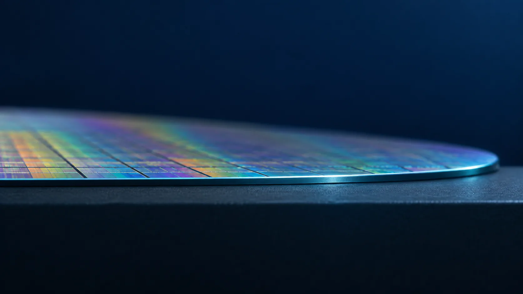
- What thinning and dicing are (the short version)
- Grinding — why thin suddenly becomes difficult
- TAIKO — the idea of leaving the rim behind
- Cutting — three methods
- Reversing the order — DBG
- A materials engineer's view: the tape is what makes this work
- What is still hard
- Glossary / Primary sources / Claim-to-source audit
Sourced = a value stated in published material from a research institute or manufacturer (link given)
Our calculation = a figure this article derived, with the assumptions spelled out
Not yet confirmed = research-stage work with no confirmed production record
Anything beyond that — how the steps fit together, and what they imply for materials design — is marked as Commentary.
1. What thinning and dicing are (the short version)
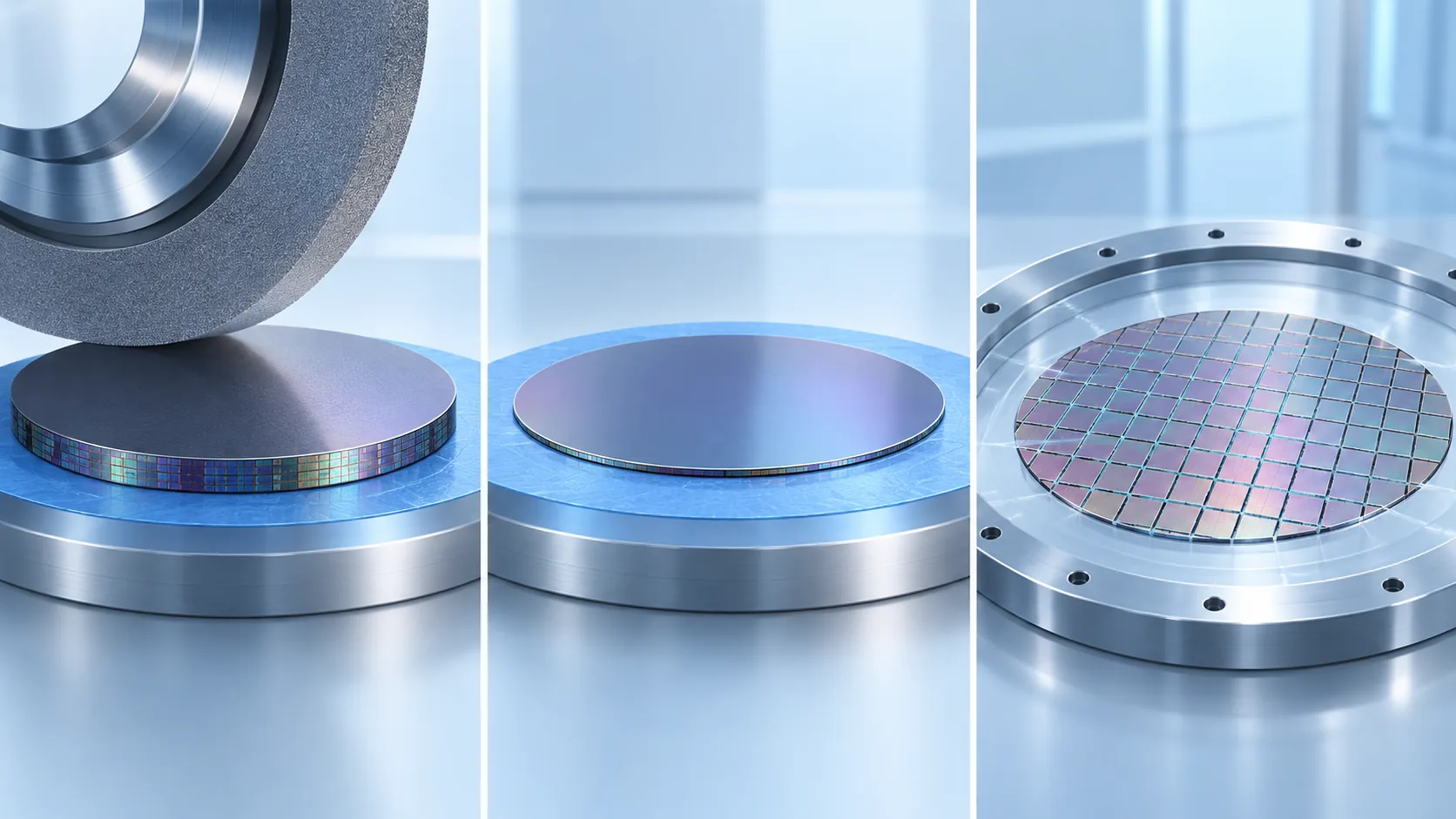
A wafer that has finished the front end of the line cannot be used as it is. At the entrance to assembly it goes through two pieces of machining.
- Thinning (backgrinding): grinding the back of the wafer to make it thinner
- Dicing (singulation): cutting the wafer into individual dies
DISCO describes its grinding technology as "thin-finish grinding that achieves wafer thicknesses of 100 µm or less at good yield"Sourced.
2. Grinding — why thin suddenly becomes difficult
Why thin a wafer at all? To stack it (see the Stacking article), to make the package thinner, and to let heat out. So what happens when you do?
The bending stiffness of a plate scales with the cube of its thicknessOur calculation.
- Assumption: take 775 µm as the usual thickness of a 300 mm wafer, and 50 µm after thinning
- Thickness ratio = 50 ÷ 775 ≈ 1/15.5
- Stiffness ratio = (1/15.5)3 ≈ 1/3,700
Assumption: 775 µm is a representative thickness for a 300 mm wafer and is a figure this article has chosen. The wafer is also treated as a simple isotropic plate.
So this is not "a bit thinner". It is three orders of magnitude less stiff. It sags under its own weight, and it cracks when you pick it up. The hard part of thinning is not the grinding. It is everything that comes after the grinding (Commentary).
3. TAIKO — the idea of leaving the rim behind
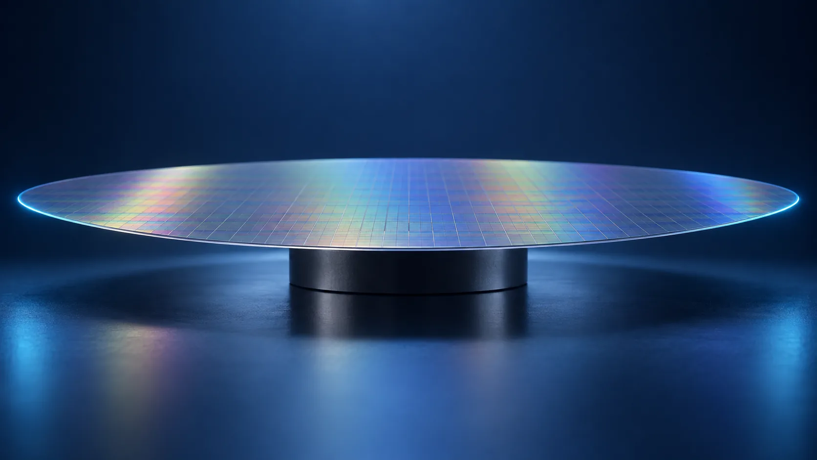
If thinning costs you three orders of magnitude of stiffness, then do not thin all of it. That is the idea behind DISCO's TAIKO process.
The company describes TAIKO as "a technology that grinds only the inner region of the wafer to thin it, leaving the outermost edge, about 3 mm wide, untouched"Sourced.
There are normally two ways to get stiffness back: change the material or make it thicker. But a wafer is silicon by definition, and thinness is the whole point. Neither route is open.
TAIKO took a third route — change the cross-section. Thin in the middle, thick only at the edge. Make it a dish with a rim and the rim carries the bending load.
Structural engineers have been doing this for a long time: the I-beam, the rolled lip of a can, the raised edge of a plate. When you cannot touch the properties of the material, the cross-section is the freedom you have left. DISCO's claim of "zero edge chipping" then follows almost trivially — there is no thin edge left to chipSourced (Commentary).
4. Cutting — three methods
There are three broad ways to separate a wafer into dies: grind it with a blade, alter it with light, or dissolve it with gas. The physics is completely different in each case.
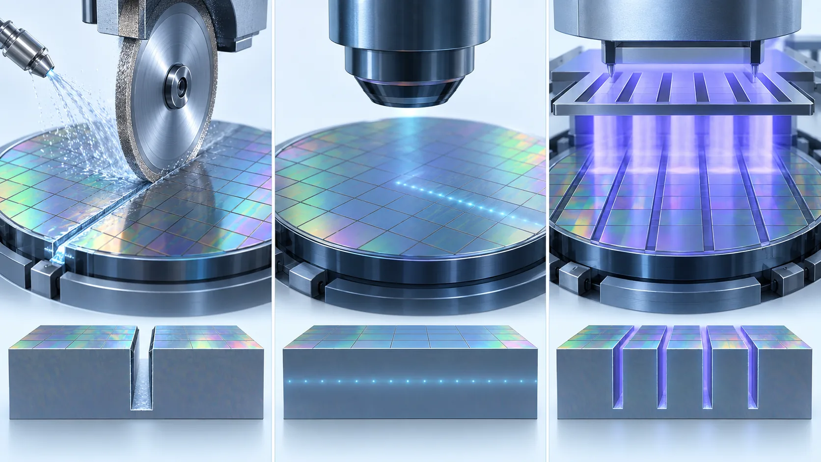
DISCO defines stealth dicing as "a dicing method in which a laser is focused inside the workpiece to form a modified layer, and the dies are then separated by expanding the tape", and lists among its benefits that "because the inside of the workpiece is modified, machining debris can be suppressed", that it is "a dry process needing no cleaning, suited to workpieces that cannot take mechanical load, such as MEMS", and that "the kerf width can be made narrower, which contributes greatly to street reduction"Sourced.
Plasma dicing is "a machining technology that singulates the wafer into dies by dry etching under vacuum", and it can "process every cut line on the wafer at the same time"Sourced.
Line the three methods up and the direction of travel is plain.
- Blade: physically grinds material away — swarf, a kerf to pay for, chipped edges
- Stealth: removes nothing, only changes the properties inside — no debris, a narrow kerf
- Plasma: turns the material into a gas by chemical reaction — neither swarf nor molten debris
The act of "cutting" is being stripped of physical removal. It is the same shape of argument as desmear in the Via article, where a chemical etch gives way to breaking the resin down with light. As features get finer, "break it and take it away" stops working (Commentary).
The phrase "process every cut line on the wafer at the same time" deserves attention tooSourced. A blade draws one line at a time, so the smaller the die, the more lines there are and the longer it takes. Process them all at once and small dies cost no extra time. That is why DISCO can say plasma dicing "maintains high UPH even for small-die devices"Sourced. The idea of "do them all at once" that the Test article described turns up here as well (Commentary).
5. Reversing the order — DBG
The Fan-out article looked at chip-first and chip-last, which is a reversal of order. Thinning and dicing have their own version of the same idea.
DISCO's DBG (Dicing Before Grinding) is "a technology that reverses the conventional sequence of backgrinding followed by wafer cutting: the wafer is half-cut first, and the dies are then separated by backgrinding"Sourced.
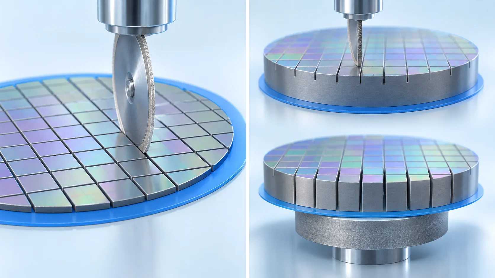
DBG solves two problems at once.
- Transport risk: the thin wafer never has to be moved (the cutting happens while it is still thick)
- Backside chipping: nothing is separated by a blade, so the back does not chip
The second of those leads straight to bending strength. A tiny chip on the back of a die is where a crack will start. Remove the chips and you get a die that is thin and still strongSourced.
What is interesting is that stealth dicing arrives at the same conclusion from the other direction. Stealth never puts a blade against the wafer at all, so again the back does not chip. One goal — do not chip the back — and two ways to reach it: solve it in the order of the steps (DBG), or solve it in the physics (stealth). There is also SDBG, which combines the two (Commentary).
6. A materials engineer's view: the tape is what makes this work
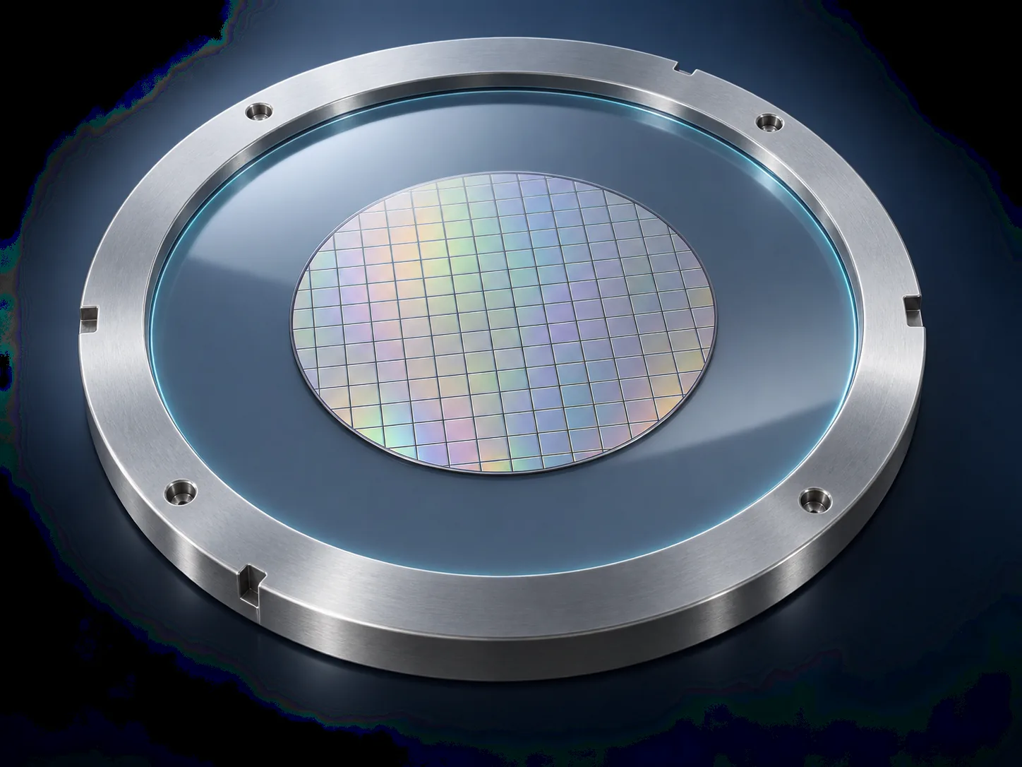
So far this has been a story about machines. But what actually holds this part of the line together is tape. LINTEC describes the jobs its semiconductor tapes do as followsSourced.
Read the description of dicing tape once more. "Before dicing, strong adhesion holds every die securely; after dicing the adhesion is weakened to make pick-up easier"Sourced.
As a specification for an adhesive, that is a strange thing to ask for.
- While cutting: withstand the blade, the force of the cutting water and the tension of tape expansion, and lose not a single die
- Once cutting is done: become weak enough that a 50 µm die can be lifted off without cracking
One material is asked to hold two opposite states, switched by time. What delivers that is a UV-curing adhesive: ultraviolet light drives crosslinking inside the adhesive and the tack drops.
This series has met the same kind of switch several times. The photosensitive resins of the Via article (react to light while you build, then never change again), and the temporary bonding materials of the PLP article (hold firmly, then release at the end). In assembly, "changing later" is sometimes the function itself — which is not something front-end materials are often asked for (Commentary).
And with dicing and die-bonding tape, the tape you cut on becomes the adhesive that fixes the die to the substrateSourced. A material that was meant to be peeled off and thrown away stays in the product. Here the line between process material and product material dissolves (Commentary).
7. What is still hard
(1) The reasons to go thinner keep multiplying
As the Stacking article showed, stacking pushes wafers thinner still. As the TSV article showed, exposing through-electrodes on the back needs thinning too. Thinning has stopped being "as thin as we can manage" and become "it only works at this thickness" (Commentary).
(2) How far can the street be narrowed?
DISCO lists among the advantages of stealth dicing that "the kerf width can be made narrower, which contributes greatly to street reduction"Sourced.
The kerf is area that never becomes a die. It feeds straight into how many dies one wafer yields. Change how you cut and you get more dies — the choice of dicing method is a yield question in disguise (Commentary).
(3) Change the material and you change the cut
DISCO lists the devices plasma dicing suits as power devices, LEDs, RFID, RF filters, MEMS and TVSSourced. It also says stealth dicing suits "workpieces that cannot take mechanical load, such as MEMS"Sourced.
Silicon, then SiC, GaN, glass, compound semiconductors — the more materials the line has to handle, the more often the cut has to be matched to the material (Commentary).
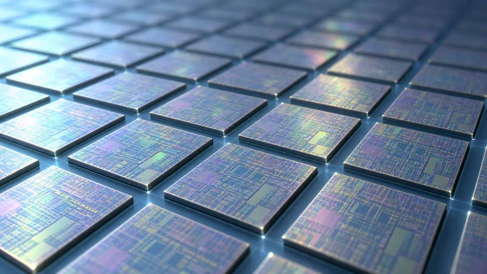
Thinning and dicing is the part of assembly where things are easiest to break outright. The countermeasures fall into three directions.
- Solve it with shape: keep the rim and keep the stiffness (TAIKO)
- Solve it with order: cut while thick, then grind to separate (DBG)
- Solve it by changing the physics: never touch it with a blade (stealth, plasma)
Underneath all three sits a tape whose adhesion changes partway through. It looks like a story about equipment and process, but in the end it is the design of the adhesive that decides whether the step is possible at all — which makes this one of the parts of assembly where materials engineers have the most to do (Commentary).
8. Glossary
- Backgrinding (BG)
- Grinding the back of the wafer to make it thinner.
- Thinning
- Reducing wafer thickness, for stacking, heat removal or thin packages.
- Dicing
- Cutting the wafer into individual dies. Also called singulation.
- TAIKO process
- Grinding only the inner region and leaving a rim of about 3 mm, to limit warpage and breakage.
- DBG
- Dicing Before Grinding. Grooves are sawn first, and backgrinding separates the dies.
- SDBG
- Stealth Dicing Before Grinding. Stealth dicing combined with DBG.
- Blade dicing
- Cutting with a thin rotating grinding wheel, the blade.
- Stealth dicing
- Focusing a laser inside the workpiece to form a modified layer, then expanding the tape to split it.
- Plasma dicing
- Singulating the wafer by dry etching under vacuum.
- Modified layer
- A layer whose internal properties have been altered by the laser. The crack starts here.
- Bosch process
- A high-aspect-ratio dry etching method developed by Robert Bosch GmbH in 1992.
- Kerf width
- The width of material lost to the cut.
- Street
- The area reserved between dies for cutting.
- Chipping
- Tiny flakes broken off during cutting. A starting point for cracks.
- Bending strength
- Resistance to bending. The measure of how easily a die cracks.
- Tape expansion
- Stretching the tape to open gaps between dies so they separate and lift off easily.
- BG tape
- Tape that protects the wafer surface during backgrinding.
- Dicing tape
- Tape that holds the dies while cutting and then releases them for pick-up.
- UV-curing type
- An adhesive that cures under ultraviolet light so its tack falls.
- DAF
- Die Attach Film. Adhesive film for fixing a die to the substrate (covered in the Underfill article).
- UPH
- Units Per Hour. How many parts are processed in an hour.
9. Primary sources
- DISCO "Grinding" (Japanese-language page) — disco.co.jp
- DISCO "TAIKO process" (Japanese-language page) — disco.co.jp
- DISCO "DBG (Dicing Before Grinding) process" (Japanese-language page) — disco.co.jp
- DISCO "Stealth Dicing™ machining" (Japanese-language page) — disco.co.jp
- DISCO "Plasma dicing" (Japanese-language page) — disco.co.jp
- LINTEC "Semiconductor-related tapes" (Japanese-language page) — lintec.co.jp
10. Claim-to-source audit
| Claim in the text | Basis | Label |
|---|---|---|
| That grinding is "thin-finish grinding that achieves wafer thicknesses of 100 µm or less at good yield" | DISCO "Grinding"[Source 1] https://www.disco.co.jp/jp/solution/library/grinding.html | Sourced |
| That the TAIKO process "grinds only the inner region of the wafer to thin it, leaving the outermost edge, about 3 mm wide, untouched". That the benefits are less wafer warpage, higher wafer strength, easier wafer handling and zero edge chipping. That 200 mm and 300 mm wafers are supported | DISCO "TAIKO process"[Source 2] https://www.disco.co.jp/jp/solution/library/grinder/taiko_process.html | Sourced |
| That DBG "reverses the conventional sequence of backgrinding followed by wafer cutting: the wafer is half-cut first, and the dies are then separated by backgrinding". That it "minimises backside chipping and wafer breakage during die separation", that "less backside chipping means thin finishing can keep a high bending strength", and that "the risk of transporting a thin wafer disappears" | DISCO "DBG process"[Source 3] https://www.disco.co.jp/jp/solution/library/dbg/dbg_process.html | Sourced |
| That stealth dicing is "a dicing method in which a laser is focused inside the workpiece to form a modified layer, and the dies are then separated by expanding the tape". That "because the inside of the workpiece is modified, machining debris can be suppressed, which suits workpieces sensitive to contamination", that it is "a dry process needing no cleaning, suited to workpieces that cannot take mechanical load, such as MEMS", and that "the kerf width can be made narrower, which contributes greatly to street reduction" | DISCO "Stealth Dicing™ machining"[Source 4] https://www.disco.co.jp/jp/solution/library/laser/stealth.html | Sourced |
| That plasma dicing is "a machining technology that singulates the wafer into dies by dry etching under vacuum". That the Bosch process was "developed in 1992 by Robert Bosch GmbH of Germany". That it can "process every cut line on the wafer at the same time". That the benefits are "high UPH even for small-die devices", "machining of many different shapes", "no swarf or molten debris" and "higher die strength". That the supported devices are power devices, LEDs, RFID, RF filters, MEMS and TVS | DISCO "Plasma dicing"[Source 5] https://www.disco.co.jp/jp/solution/library/other/plasma.html | Sourced |
| That BG surface protection tape "reliably protects the wafer surface during backgrinding and prevents contamination of that surface by grinding water and swarf". That dicing tape holds every die with strong adhesion before dicing and weakens afterwards to make pick-up easier. That dicing and die-bonding tape is "a high-value-added tape combining the functions of a dicing tape and a die-bonding adhesive". That die backside protection tape was "developed to protect and reinforce the back of the die in applications such as flip chip, where the die is mounted circuit-face down" | LINTEC "Semiconductor-related tapes"[Source 6] https://www.lintec.co.jp/products/electronics/tape/ | Sourced |
| Taking bending stiffness as proportional to the cube of thickness, the values relative to 1 at 775 µm (350 µm gives about 1/12, 100 µm about 1/460, 50 µm about 1/3,700) | Our calculation. 775 µm is a representative thickness for a 300 mm wafer that this article has chosen, not the specification of any particular product. The wafer is treated as a simple isotropic plate, so crystal orientation, residual stress and the damaged subsurface layer are not included | Our calculation |
| The drawbacks listed for blade dicing (a kerf is needed, the back chips, cleaning is required) | Commentary: this article framed them as the flip side of the advantages DISCO claims for stealth and plasma dicing. DISCO does not state them as drawbacks of blade dicing | Commentary |
| The reading that TAIKO secured stiffness through cross-sectional shape rather than material or thickness. The framing that cutting is moving away from physical removal. The explanation that crosslinking in a UV-curing adhesive lowers its tack. The observation that "changing later" is itself a required function. The observation that the line between process material and product material dissolves. The observation that kerf width feeds straight into die count per wafer | Commentary by this article, based on published material. Not positions stated by any of the companies | Commentary |
| That the cross-sections in Figs. 1, 4, 5 and 6 are explanatory drawings rather than observed images | Our note | Commentary |
Last updated 20 September 2026. Sources are limited to primary material (official technical pages from equipment and materials manufacturers). Because this article also organises the process and reads it from a materials-design angle, those passages are marked as Commentary and kept apart from sourced fact. All figures are explanatory concept graphics. Visual-overview figures are shown as AI-generated conceptual images, matching the Japanese edition. Vector drawings are retained where they carry quantitative values or precision-critical technical labels. AI-generated images do not depict real equipment, products, facilities, dimensions or exact cross-sections; replaced source SVG overview drawings remain in the HTML but are hidden.