TECHNOLOGY EXPLAINER
EMIB and EMIB-T
— a silicon bridge buried in the substrate, and now a power path through it
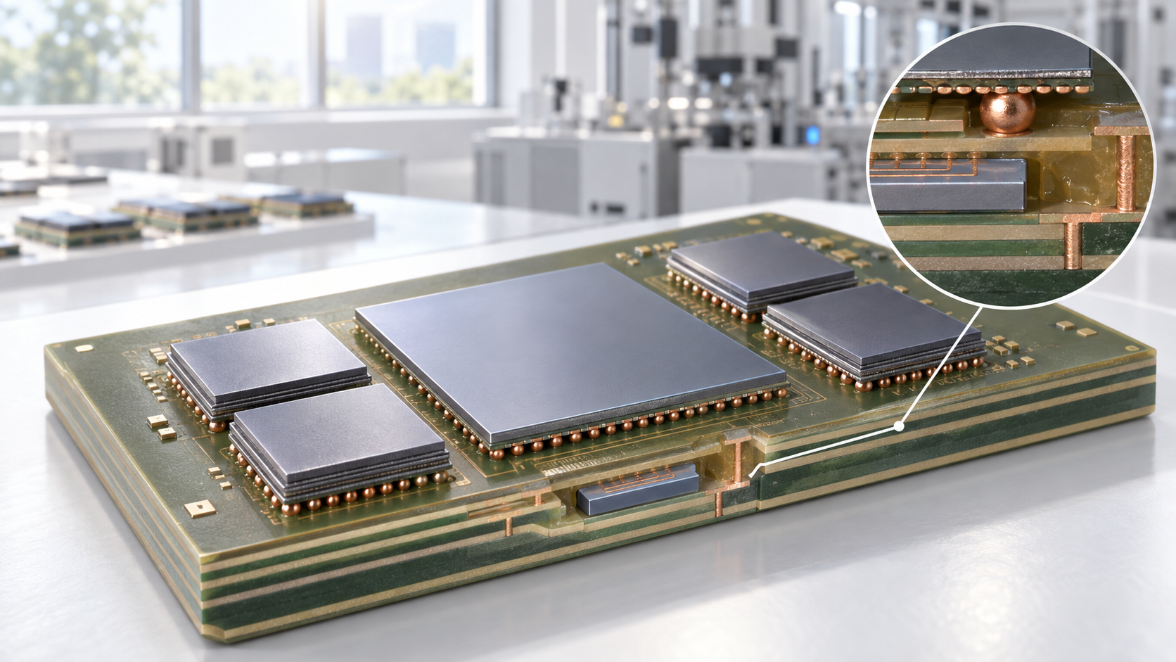
EMIB (Embedded Multi-die Interconnect Bridge) is Intel's packaging technology in which a small silicon bridge is embedded in a cavity of an organic substrate and links neighboring chips with fine wiring. Intel says EMIB has been in volume production since 2017. EMIB-T adds through-silicon vias (TSVs) to that bridge, so that power can be delivered from directly beneath it. This article separates what Intel's announcements, conference papers and published patents let us confirm from what we could not confirm.
- What EMIB and EMIB-T are (the short version)
- What came first, and when — from the idea to today
- Structure — buried in the substrate, wired out from above
- EMIB-T — why put TSVs through the bridge
- Embedding the bridge: process steps and materials issues
- A materials engineer's view: the difficulty moved to the substrate side
- How big can it get — multiples of the reticle
- Our calculation: HBM4 and HBM4E bandwidth
- Foveros, EMIB 3.5D and Intel's other technologies
- Availability to outside customers (Intel Foundry)
- What we could not confirm
- Glossary / References / Claim-to-source audit
Sourced = stated in published material (company announcements, conference papers, published patents), with a link
Our calculation = a figure this article derived, with the assumptions spelled out
Not yet confirmed = a plan or a target with no confirmed track record
Structural readings and materials-design interpretations are marked separately as Commentary.
Customer names, production timing and yield figures that appear only in news reports are not used here.
1. What EMIB and EMIB-T are (the short version)
EMIB is a technology that buries a small silicon bridge in a cavity of the substrate and connects only the facing edges of neighboring chips with fine wiring. EMIB-T is the version in which TSVs have been added to that bridge.
- What EMIB is: Intel calls it "the industry's first 2.5D interconnect solution using bridges embedded in the substrate." The bridge sits in a substrate cavity held in place with adhesive, and dielectric and metal build-up layers are then added on top [Ref. 1] Sourced
- What EMIB-T is: Intel says that, because demand for high-bandwidth memory (HBM) raised the need for vertical power delivery with minimal DC and AC noise, Intel Foundry added TSVs to EMIB-T [Ref. 1]. An Intel conference paper describes a direct power-delivery path through the bridge, from the package bottom to the ASIC and the HBM [Ref. 18] Sourced
- Where it stands: EMIB has been in volume production since 2017 [Refs. 1, 2] Sourced. EMIB-T was announced as a new offering in April 2025 [Ref. 5], and a 2026 conference paper reports on the reliability of a "1st generation" during initial development [Ref. 18] Sourced. We could not find a primary source showing that EMIB-T has entered volume production. Not yet confirmed
EMIB = Embedded Multi-die Interconnect Bridge [Ref. 1]. An Intel patent filed in 2013 uses the older name Embedded Interconnect Bridge (EmIB) [Ref. 20] Sourced.
EMIB-M = the bridge incorporates MIM (metal-insulator-metal) capacitors to strengthen power delivery [Ref. 1] Sourced.
EMIB-T = the bridge incorporates TSVs. The 2026 ECTC papers write "Embedded multi-die interconnect bridge with through-silicon vias" [Refs. 16, 17], and an Intel Foundry blog writes "Embedded Multi-die Interconnect Bridge-T" [Ref. 3]. According to another Intel Foundry blog, EMIB-T has MIM capacitors in addition to the TSVs [Ref. 4] Sourced.
EMIB 3.5D = EMIB and Foveros combined in a single package [Refs. 1, 2] Sourced.
The basics of EMIB (how it differs from a full silicon interposer, the dual bump pitch that is fine only above the bridge, the assembly flow, and the existence of EMIB-M and EMIB-T) were covered in our explainer on bridges. This article does not repeat that material and instead concentrates on the following.
- How EMIB was introduced, and the order in which it entered products
- What changed with EMIB-T (the TSV power path and the published specifications)
- Materials issues in embedding the bridge in a substrate (cavity formation, adhesion, build-up, thermal expansion mismatch, warpage)
- How EMIB relates to Foveros, EMIB 3.5D and Intel's other technologies, and what is known about its availability to outside customers
See our explainers on interposers and CoWoS (CoWoS-L) for full-sheet silicon interposers, on TSVs for how TSVs are made, on chiplets for chiplets in general, on package substrates and build-up film for substrate lamination, on the coefficient of thermal expansion for expansion mismatch, and on glass substrates for future substrate materials.
2. What came first, and when — from the idea to today
Ravi Mahajan, the Intel engineer known as the developer of EMIB, described the history in an Intel interview published in May 2026. In the early 2000s the team asked whether packaging had its own scaling roadmap, concluded that interconnect density was a key limit, and explored putting silicon interconnect directly into the package. In his words, "By 2013, we were confident enough to bring EMIB into a production program and then introduced it to the public the following year" [Ref. 6] Sourced. He adds that the idea was simple but "required solving complex challenges in materials, stress management, and manufacturing" [Ref. 6] Sourced.
| When | What was published | Status |
|---|---|---|
| 2013-2014 | According to the developer, the team gained confidence to take EMIB into a product program in 2013 and made it public the following year [Ref. 6] | Sourced |
| 8 June 2015 | Altera announced that initial Stratix 10 devices would use EMIB to integrate high-speed serial transceiver and protocol tiles with monolithic core logic, and said EMIB offers higher performance, reduced complexity, lower cost and enhanced signal integrity compared with interposer-based approaches (at the time, a forward-looking statement) [Ref. 10] | Sourced |
| May 2016 | Mahajan et al. presented an overview of EMIB's architecture, assembly process and bandwidth at ECTC 2016, citing as advantages that it needs no TSVs and can support many large die over an area much greater than the reticle limit [Ref. 13] | Sourced |
| 6 November 2017 | Intel announced a product combining a Core processor, HBM2 and a custom graphics die from AMD in one package, and called it "the first consumer product that takes advantage of EMIB" [Ref. 9] | Sourced |
| 2017 onward | Intel states EMIB has been in volume production since 2017, with both Intel and external silicon [Refs. 1, 2] | Sourced |
| October 2019 | A TCPMT paper by Mahajan et al. showed implementation examples (FPGA with HBM2, graphics die with HBM2, and others) and put the interconnect density at 500-1000 I/O/mm [Ref. 14] | Sourced |
| 19 August 2021 | At Architecture Day 2021, Intel described Sapphire Rapids as a tiled SoC that leverages EMIB, and Ponte Vecchio as tiles joined through an EMIB tile [Ref. 11] | Sourced |
| June 2024 (document date) | An Intel quality and reliability paper says that with 2nd-generation EMIB the bump pitch was reduced from 55 to 45 microns [Ref. 12] | Sourced |
| 29 April 2025 | At Intel Foundry Direct Connect, Intel announced EMIB-T among its new advanced packaging offerings, along with a new engagement with Amkor [Ref. 5] | Sourced |
| July 2025 | Intel published the EMIB Technology Brief, which covers EMIB-M and EMIB-T [Ref. 1]. A TED paper organized EMIB's expansion along four vectors: pitch and wire scaling, TSVs in the bridge, an open-cavity architecture, and active bridge die [Ref. 15] | Sourced |
| March and May 2026 | IRPS 2026 carried a reliability characterization of 1st-generation EMIB-T [Ref. 18]. ECTC 2026 carried papers on scaling EMIB-T and on signal quality above 12 Gb/s for HBM4E [Refs. 16, 17] | Sourced |
| 2026-2028 | Intel aims for EMIB-T complexes of more than 8x the reticle size (2026) and more than 12x (2028) [Ref. 3] | Not yet confirmed |
* The April 2025 item is an announcement of a new offering. An Intel newsroom article of July 2026 also says that "in 2026 the latest development is EMIB-T" [Ref. 7], but that sentence alone does not establish a date, so this article uses the 29 April 2025 announcement.
One question worth asking is which product was first. Intel's 2017 announcement does say "first consumer product" [Ref. 9], but we could not find a primary source that settles which product, counting data-center parts and FPGAs, came first. Altera's 2015 announcement was a forward-looking statement about Stratix 10 [Ref. 10], and the actual shipment date is not confirmed in the sources we reviewed.
3. Structure — buried in the substrate, wired out from above
In EMIB the silicon bridge sits in a cavity of an organic substrate, build-up layers are formed over it, and vias connect to fine pads on the bridge. The two neighboring chips sit on fine bumps directly above the bridge, near their facing edges (for how this differs from a full-sheet interposer, see our explainer on bridges). Here we gather what the primary sources reveal about materials and how it is made.
- Bridge substrate material: an Intel patent filed in 2012 (granted in 2014) says the bridge substrate may be glass or a semiconductor such as high-resistivity silicon, with electrical routing formed on it. The bridge is placed in a cavity formed in the package substrate, and an example is given in which a die-attach adhesive couples the bridge substrate to the epoxy material of the package substrate [Ref. 19] Sourced
- How fine the wiring is: the background section of another Intel patent says EMIB uses a silicon piece carrying ultrafine line-and-space structures (for example 2 µm / 2 µm), which can be fabricated with silicon back-end-of-line technology but are beyond the capability of organic substrate manufacturing. One or more such pieces are embedded in a cavity skived into a standard organic substrate and bridge the fine bump-pitch areas between dies (55 µm pitch is given as an example) [Ref. 21] Sourced
- No TSVs (in conventional EMIB): the 2016 paper lists among EMIB's advantages that it provides high-density interconnect cost-effectively without TSVs, and that it can support many large die over an area much greater than the reticle limit [Ref. 13]. The 2019 paper puts the interconnect density at 500-1000 I/O/mm and says the link is realized while leaving the rest of the package structures and designs unaffected [Ref. 14] Sourced
Read literally, the patent's statement (2 µm-class wiring is made with silicon BEOL because it lies outside what organic substrate manufacturing can do) means that EMIB hands the finest wiring to the silicon factory and leaves the substrate factory with a different set of jobs: forming a cavity, placing and fixing the piece, wrapping it in resin and connecting to it from above (our commentary). Materials development for the finest wiring (insulating films, barrier metals, copper) is therefore a silicon-side matter, while the substrate-side materials issues are cavity machining, adhesion, filling with build-up resin, and thermal expansion mismatch. Sections 5 and 6 take these up.
4. EMIB-T — why put TSVs through the bridge
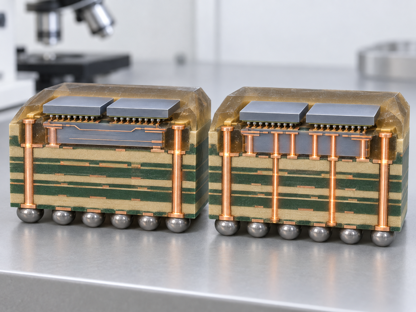
Conventional EMIB bridges had no TSVs. The background section of an Intel patent filed in 2013 says: "unlike silicon interposers, the embedded interconnect bridge die does not have through-silicon vias to enable power connections from outside the package to the bridge. This is in part because of the very thin structure of such a bridge" [Ref. 20] Sourced. With no vertical path beneath the bridge, power has to reach the chips by passing around it (our commentary, consistent with Intel's own wording "instead of around it" [Ref. 7]).
EMIB-T adds the TSVs. Intel says it did so because demand for HBM has increased "the need for vertical power delivery with minimal DC and AC noise" [Ref. 1] Sourced. An Intel newsroom article of July 2026 describes EMIB-T as adding "channels through that bridge to deliver power directly to the chips, instead of around it" [Ref. 7] Sourced.
| Name | What is added to the bridge | Intel's description | Status |
|---|---|---|---|
| EMIB | (base form) | Silicon bridge embedded in the substrate, connecting adjacent die; used for logic-to-logic and logic-to-HBM links [Refs. 1, 2] | Sourced |
| EMIB-M | MIM capacitors | Incorporates MIM capacitors into the silicon bridge to enhance power delivery [Ref. 1]; optimizes I/O signal integrity and power delivery [Ref. 4] | Sourced |
| EMIB-T | TSVs (and MIM capacitors) | Adds TSVs in addition to MIM capacitors to meet the greater bandwidth and power needs of HBM and UCIe products [Ref. 4]. This architecture also enables design conversion from other packaging technologies [Refs. 1, 2] | Sourced |
* On design conversion, Intel says only that EMIB-T "can ease the enablement of IP integration from other packaging designs" and does not explain how [Ref. 2].
Published EMIB-T numbers, and the conditions behind them
| Item | Value | Source and conditions | Status |
|---|---|---|---|
| FLI bump pitch | Scaled to 25 µm | ECTC 2026 Intel paper [Ref. 16]. FLI = First Layer Interconnect (the die-to-package connection). Intel's blog says this was "demonstrated" [Ref. 8]. For reference, 2nd-generation EMIB is 45 µm [Ref. 12]. Use in a product could not be confirmed | Sourced |
| Package size | Over 120 mm × 120 mm | Same paper. Hosts more than 9x reticles of compute and memory silicon on one package [Ref. 16] | Sourced |
| HBM4E signaling | Over 12 Gb/s | Wideband electrical measurements correlated with models; signal and power integrity optimization confirms the feasibility of 12+ Gb/s operation [Ref. 17]. Intel's blog also cites 64 Gb/s UCIe interface performance [Ref. 8] | Sourced |
| Reliability | 1st-generation EMIB-T | IRPS 2026. Reports thermo-mechanical reliability data from pathfinding test vehicles, with observed fail mechanisms and improvements. We could not read the paid full text, so no figures are given [Ref. 18] | Sourced |
| Planned reticle multiples | Over 8x in 2026, over 12x in 2028 | Intel Foundry blog. The 2028 case is about 10,000 mm², 16 or more HBM4/HBM5 stacks and 30 or more EMIB-T bridges [Ref. 3] | Not yet confirmed |
* Bridge dimensions and thickness, TSV diameter, pitch and count, the start of volume production, and the names of products using EMIB-T could not be confirmed from the primary sources we reviewed. Some news reports give a package size of "120 mm × 180 mm", but we could not confirm it in primary sources and do not use it.
The patent filed in 2013 gave the thinness of the structure as part of the reason for having no TSVs [Ref. 20] Sourced. More than a decade later, TSVs are in the same kind of bridge in EMIB-T. What changed to make that possible is not explained in the published material. We could not confirm the bridge thickness, the TSV diameter and aspect ratio, the insulating film / barrier / copper stack, or the thinning and TSV-reveal steps.
A bridge with through-holes is not a new idea on paper: a patent filed in 2012 describes bridge substrates with through-hole vias (TSVs, if the bridge is silicon) as embodiments, for example for bringing out a ground connection [Ref. 19] Sourced.
Whether that matches the structure of today's EMIB-T could not be confirmed.
What we can confirm is the picture: vertical copper (TSVs) inside a piece of silicon that is itself buried in an organic substrate.
As our explainer on TSVs showed, copper expands more than silicon on heating and loads its surroundings. In EMIB-T the counterparts of that stress are not only the silicon but also the adhesive, the build-up resin and the substrate core.
That the IRPS 2026 paper deals with "thermo-mechanical reliability data" and "observed fail mechanisms" [Ref. 18] suggests this chain is where the difficulty lies (our commentary; the actual failure modes are unconfirmed).
5. Embedding the bridge: process steps and materials issues
Intel states that the EMIB assembly flow is a standard semiconductor package-assembly flow, "with the only difference being the manufacturing of the substrate" [Ref. 1] Sourced. So the materials and process issues concentrate on the part where a piece of silicon is buried in the substrate. Below we split that part into five steps using Intel's technical document plus the background and embodiments of Intel's published patents. A patent says "this is the problem, and this is a way it could be solved"; it does not describe the current production process.
(1) Forming the cavity: laser or lithography
The background of an Intel patent (filed 2018, granted 2022) describes the limits of today's cavity formation as follows [Ref. 21] Sourced.
- The cavity is made by laser-skiving a standard organic substrate.
- Bump pitch is projected to go to 30 µm or lower, while bump thickness variation must stay below 10 µm for assembly.
- But "multi-layer organic substrates can have thickness variation of over 40 µm even before reaching the final layer." The layer thickness the laser has to skive is not uniform and varies within a lot and even within a panel, so there is a higher chance of laser punch-through that damages the underlying copper pads.
- Cavity dimensional and location tolerances must improve when smaller silicon bridges are used.
The same patent adds that the trepanning method, in which laser shots are overlapped, produces misalignment between shots as the galvanometer moves, gives a wave-like perimeter, and that locations with maximum spot overlap take a larger thermal hit and are more prone to copper-pad delamination [Ref. 21] Sourced. As an alternative, it presents embodiments in which the cavity is defined lithographically.
| Aspect | Laser skiving (as described in the patent background) | Lithographic definition (patent embodiment) |
|---|---|---|
| How the cavity is made | The dielectric layer is ablated with laser shots | Sacrificial copper blocks are formed at the same time as pads and pillars, covered by a layer and planarized, then etched away to leave the cavity |
| Size and position | Shot-to-shot misalignment; wave-like perimeter | Set by the same mask as the other conductors; embodiments with a tolerance of about ±3 µm |
| Effect on copper pads | Prone to punch-through from layer-thickness variation, and to heat-induced delamination | Described as having no risk of copper punch-through |
| Remaining issues | Tolerances get tighter as pitch shrinks | A stepped cavity (an overhang) may reduce reliability if the cavity cannot be fully filled. A cavity without a step relaxes the design rules of the conductor layers because of the resolution limit of thick resist |
All Sourced (background and embodiments of Intel patent US 11,322,444 B2 [Ref. 21]). We could not confirm whether this approach is used in any product.
(2) Placing and fixing the bridge
The patent shows an embodiment in which the bridge is fixed to the floor of the cavity with an adhesive such as a die bond film (DBF) [Ref. 21]. A patent filed in 2012 likewise shows the bridge substrate bonded to the epoxy material of the package substrate with a die-attach adhesive or similar [Ref. 19] Sourced. The embodiments also give the following numbers [Ref. 21] Sourced.
- Example cavity width: about 10 mm (any size is allowed as long as it holds the bridge)
- Gap G between the bridge sidewall and the cavity sidewall: embodiments of 100 µm or less, 50 µm or less, and 20 µm or less
- The bridge is thinner than the layer containing the cavity, so its top surface lies below the substrate surface in the first embodiments (coplanar and protruding cases are also described)
- Wiring on the bridge: line/space of 10/10 µm or less, and further 2/2 µm or less
(3) Wrapping in resin: gaps and voids
A build-up layer (the "third layer") is then formed over the bridge, fills the gap around it, and covers its sidewalls and top surface [Ref. 21] Sourced. Intel's technical document likewise says dielectric and metal build-up layers are added in this step [Ref. 1] Sourced. The patent itself notes that a cavity with a stepped overhang may be less reliable if the cavity cannot be fully filled [Ref. 21] Sourced.
From a materials standpoint this is the problem of filling a narrow gap, tens to a hundred micrometers wide, with build-up resin without voids (our commentary). Film flow and thickness uniformity are covered in our explainer on build-up film, and gap filling in our explainer on underfill.
(4) Bringing the wiring out, then mounting the chips
Fine pads on the bridge are connected through vias opened in the third layer [Ref. 21] Sourced. Because the bridge is buried and invisible, the accuracy with which the vias land on the pads of the bridge is tied to the positional tolerance of the cavity (our commentary). The bump pitch for the chips that go on top was reduced from 55 µm to 45 µm with 2nd-generation EMIB [Ref. 12] and has been reported scaled down to 25 µm for EMIB-T [Ref. 16] Sourced. For the joining and filling materials, see our explainers on bumps and underfill.
6. A materials engineer's view: the difficulty moved to the substrate side
The bridge approach avoids the difficulties of a full sheet of silicon (large area, TSVs, thinning) but takes on those of a joint between dissimilar materials inside the substrate. This section takes up three that can be examined with numbers.
(1) Expansion mismatch, expressed as a length
Around the bridge, silicon, adhesive and build-up resin are in contact. We estimate the difference in expansion as an upper bound for free expansion Our calculation.
- Assumption: bridge length 10 mm (the example cavity width in the patent [Ref. 21]; not the size of any real product's bridge)
- Assumption: CTE of silicon 3.4 ppm/K (the convention in our explainer on the coefficient of thermal expansion, borrowed from the value for the LTCC that Kyocera describes as close to silicon [Ref. 26])
- Assumption: CTE of the surrounding resin 24.5 ppm/K (Sekisui Chemical's interlayer insulation film NX04H, 25-150 °C [Ref. 25])
- Assumption: temperature change 235 K (260 °C to 25 °C, as in that explainer)
- CTE difference = 24.5 − 3.4 = 21.1 ppm/K
- Difference in expansion = 10 mm × 21.1 ppm/K × 235 K = 10 mm × 0.00496 = about 0.050 mm (about 50 µm)
- Ratio to the cavity tolerance example (±3 µm) = 50 ÷ 3 ≈ about 17
Assumptions and limits: a real bridge is bonded and constrained by the resin, so it does not expand freely. The 50 µm does not become displacement; it means that the mismatch remains as stress instead. The in-plane expansion of the whole substrate is also dominated by the core material (which, as our explainer shows, is low in-plane) and is a separate matter from the build-up resin value. The CTE of the resin also changes around its Tg and with direction. All this calculation shows is that the order of magnitude (tens of micrometers) of the mismatch around the bridge lies in the same range as the cavity gap (20-100 µm) and well above the tolerance (a few micrometers).
(2) How Intel approaches reliability testing
Intel's quality and reliability paper (June 2024) says advanced packages such as Foveros and EMIB require a more complex verification process [Ref. 12] Sourced. On temperature cycling it explains that "thermo-mechanically induced damage results from differences in the material properties of the constituent materials over the range of cycling temperatures," and lists solder-joint fatigue, package cracking, and interlayer-dielectric (ILD) cracking in the die and package as accelerated failure mechanisms [Ref. 12] Sourced. As example conditions it gives temperature cycling between 125 °C and −55 °C per JEDEC JESD22-A104, and an unbiased highly accelerated stress test (HAST) at 110 °C and 85% relative humidity per JESD22-A118. These are stated as examples and are not specification values for EMIB or EMIB-T [Ref. 12] Sourced.
(3) The variables researchers are looking at
Third-party finite-element work on EMIB reports the following. It is an analysis by Zhou and Wang of Fudan University with a 165 °C temperature rise applied [Ref. 22] Sourced.
- A bump diameter-to-pitch ratio of 0.3 optimizes the stress distribution
- A peripheral bump arrangement is better at reducing stress than other patterns
- The thinner the EMIB (bridge), the lower the maximum principal stress, linearly
- The number of EMIBs and the aspect ratio have minimal effect
These are results for a generalized model and not values for any specific product. One could read from them that thickening the bridge to accommodate TSVs might work against stress, but whether EMIB-T bridges are thicker than before is not confirmed (our commentary).
A different approach, which embeds the bridge in an organic redistribution layer (RDL), is discussed by ASE under the name fan-out embedded bridge. ASE says that small, thin silicon bridges and power components can exacerbate warpage during package assembly, that high warpage can lead to defects such as non-contact open, bridge, non-wet or stretch joints, and that controlling warpage is therefore crucial for OSATs [Ref. 27] Sourced. This is a structure different from EMIB; we cite it only because the same classes of defects are named as shared concerns of embedded-bridge approaches. Intel also lists, among its ECTC 2026 presentations, one on the creep behavior of assembly materials and its effect on package warpage, but we could not confirm the content [Ref. 8] Sourced.
Lining up the numbers from the patent, the substrate-side issues can be grouped into three mismatches (our commentary).
- Thickness mismatch: the thickness variation of multilayer organic substrates (over 40 µm) against the allowed variation in bump height (under 10 µm). Because the layer the laser skives is not uniform, it does not stop at the depth you want
- Position mismatch: the tolerance on cavity size and position (an example of ±3 µm with lithography), shot-to-shot misalignment, and the alignment of vias to pads on the bridge
- Expansion mismatch: the CTE difference between silicon and resin (about 50 µm per 10 mm in our estimate). It is constrained and becomes stress that gathers at the adhesive interface, the TSVs and the fine wiring
As the pitch shrinks from 45 µm to 25 µm, all three tolerances must tighten together. The levers on the materials side include layer-thickness uniformity (control of films and lamination), the modulus and CTE of adhesives and resins (stress relief), and the metal and etch selectivity of any sacrificial layer, but which materials Intel actually chooses, and how, has not been published. Read less as a "materials datasheet" problem and more as a question of who carries which tolerance, it shows what is likely to be contested among substrate makers, materials suppliers and OSATs.
7. How big can it get — multiples of the reticle
The metric EMIB-T puts forward is how many reticle fields of silicon one package can carry. Intel Foundry's blog (March 2026) explains that an interposer larger than one reticle has to be made by reticle stitching, which is complex and expensive, and that silicon bridges embedded in the substrate are a more cost-effective alternative [Ref. 3] Sourced. It then gives the following scale for EMIB-T.
- Today: die complexes of more than 6x the reticle size [Ref. 3] Sourced
- 2026: more than 8x (about 6,800 mm²) [Ref. 3] Not yet confirmed
- 2028: more than 12x (about 10,000 mm²), using 16 or more HBM4/HBM5 stacks and 30 or more EMIB-T bridges [Ref. 3] Not yet confirmed
- ECTC 2026 paper: more than 9x reticles of silicon on a package larger than 120 mm × 120 mm [Ref. 16] Sourced
* An Intel newsroom article of July 2026 says it is "scaling packages to 8x the industry standard today, and over 12x by 2028" [Ref. 7]. The March 2026 blog says more than 6x today and more than 8x this year [Ref. 3]. Because the dates and the baseline are worded differently, this article follows the breakdown in the March blog and treats 8x as a target for 2026.
We combine the published figures into a few conversions Our calculation.
- Area of one reticle (back-calculated): 6,800 mm² ÷ 8 = 850 mm², and 10,000 mm² ÷ 12 ≈ 833 mm². Working back from Intel's "about" figures, one reticle is roughly 830-850 mm²
- Silicon area in the paper (rough): 850 mm² × 9 = at least about 7,650 mm²
- Package area: 120 mm × 120 mm = more than 14,400 mm²
- Share: 7,650 ÷ 14,400 ≈ about 53%
Assumptions and limits: "more than 9x" and "over 120 mm square" are both lower-bound statements, so the ratio is only a guide. The area of one reticle is back-calculated from figures Intel gives as "about". Even so, it indicates that even in the largest EMIB-T packages, roughly half of the package area is substrate (organic material) (our commentary). The share of silicon does not approach 100%, and the flatness and warpage control of a large organic substrate matter more as the scale grows.
Intel's account of how the manufacturing flow differs from an interposer
Intel Foundry's blog describes the difference in manufacturing flow as follows [Ref. 3] Sourced.
- In EMIB-T, small silicon bridges are fabricated on a wafer at very high density, giving about 90% wafer utilization. The bridges are then embedded in large-format organic rectangular panels, which are singulated.
- A full-size interposer, by contrast, has to be fabricated over the whole package footprint on a wafer, and for complexes of more than 8x the reticle this "can reduce wafer utilization to as low as 60%."
- Intel says the EMIB-T flow is well aligned with panel-based manufacturing.
This is Intel's account and does not rank EMIB against other approaches. Intel also says that bridge-based packaging from other foundries, which places local silicon interconnect (LSI) bridges in the interposer, needs more assembly steps [Ref. 3]; for the structural difference, see CoWoS-L in our CoWoS explainer. This article does not judge which is better.
If Intel's account holds, what grows with EMIB-T's scale is the area of organic substrate (in the calculation above, about half of the package even at the largest size). The issues we met in our explainers on package substrates, build-up film and thermal expansion — flatness, warpage, layer registration, and uniformity of build-up resin — then become the wall that scale runs into (our commentary).
Intel itself says organic core substrates are reaching their limit for scaling, and that it is researching glass core substrates [Refs. 4, 8] Sourced. It also says that "while organic substrates warp and shift during processing, glass stays flat and stable" [Ref. 8], but this is research-stage work with no timeline for practical use Not yet confirmed (see our explainer on glass substrates).
8. Our calculation: HBM4 and HBM4E bandwidth
The EMIB-T paper states that operation above 12 Gb/s is feasible for HBM4E [Ref. 17] Sourced. The JEDEC HBM4 standard specifies a 2048-bit interface at up to 8 Gb/s, and up to 2 TB/s per stack [Ref. 24] Sourced. We combine the two.
Our calculation
- HBM4 (8 Gb/s): 2,048 × 8 Gb/s = 16,384 Gb/s = 2,048 GB/s ≈ 2 TB/s per stack (matches the JEDEC figure)
- HBM4E (12 Gb/s, assuming 2,048 bits): 2,048 × 12 Gb/s = 24,576 Gb/s = 3,072 GB/s ≈ 3.1 TB/s per stack
- With 16 stacks: at 8 Gb/s, 2,048 GB/s × 16 = 32,768 GB/s ≈ 33 TB/s; at 12 Gb/s, 3,072 GB/s × 16 = 49,152 GB/s ≈ 49 TB/s
- Edge length of bridge needed: carrying 2,048 data lines at 500-1000 I/O/mm [Ref. 14] takes 2,048 ÷ 1000 ≈ 2.0 mm to 2,048 ÷ 500 ≈ 4.1 mm (data lines only, a rough figure)
Assumptions and limits: the abstract of the paper we reviewed does not give the interface width for HBM4E, so we assumed 2,048 bits as for HBM4. "16 stacks" uses Intel's plan for 2028 (16 or more HBM4/HBM5 stacks) as an arithmetic example; we do not cover the HBM5 specification here. The 12 Gb/s result is a stage at which operation was confirmed feasible through signal- and power-integrity optimization [Ref. 17]; it is not the performance of a product. The 500-1000 I/O/mm range is what the 2019 paper gave for the EMIB examples of that time [Ref. 14], and we could not check in the paid full text how it is defined (signals only or including power, and how many layers). Clock, command and power wiring are not included.
In other words, the fast signals of one HBM stack cross a few millimeters of bridge edge. One can read the small size of the bridge as resting on numbers of this order (our commentary).
9. Foveros, EMIB 3.5D and Intel's other technologies
Intel's packaging technologies can be sorted into lateral (2.5D) and vertical (3D). EMIB connects chips sideways and Foveros stacks them. Using both gives EMIB 3.5D. Intel describes EMIB 3.5D as a hybrid that combines the vertically stacked chiplets of Foveros with the silicon-embedded bridge of EMIB in a single package, and says it addresses "the downsides of thermal warping, reticle size limits, and interconnect constraints" [Ref. 1] Sourced.
| Name | Structural point | Intel's description | Status |
|---|---|---|---|
| EMIB 2.5D | Silicon bridge embedded in the package substrate; a "shoreline-to-shoreline" connection | In mass production since 2017, with Intel and external silicon [Ref. 2] | Sourced |
| EMIB-M / EMIB-T | MIM capacitors / TSVs added to the bridge | See section 4 [Refs. 1, 2, 4] | Sourced |
| Foveros-S 2.5D | Silicon interposer with 4x reticle, with an active base die | For client applications; in mass production since 2019 [Ref. 2] | Sourced |
| Foveros-R 2.5D | RDL interposer | For client and cost-sensitive segments. "Production ready in 2027" [Ref. 2] | Not yet confirmed |
| Foveros-B | Integrates bridges; for larger HPC applications needing higher routing density | Announced in April 2025 with Foveros-R as a new offering [Refs. 4, 5]. Production timing could not be confirmed | Sourced |
| Foveros Direct 3D | Stacks chiplets on a base die by Cu-to-Cu hybrid bonding (HBI) | Used within EMIB 3.5D configurations [Ref. 2] | Sourced |
| EMIB 3.5D | EMIB and Foveros in one package | Intel Data Center GPU Max: more than 100 billion transistors, 47 active tiles, 5 process nodes [Ref. 2] | Sourced |
* The "2027" for Foveros-R is a "production ready" date and is a plan. The production timing of Foveros-B could not be confirmed. Intel describes Sapphire Rapids as a tiled SoC leveraging EMIB, and Ponte Vecchio as tiles joined through an EMIB tile and assembled with Foveros packaging [Ref. 11].
Intel's quality and reliability paper describes EMIB as providing high-bandwidth connectivity between multiple large chiplets without a silicon interposer, and says it can also connect multiple compute modules made with Foveros Direct 3D, a combination called EMIB 3.5D [Ref. 12] Sourced. It adds that this allows systems with a total silicon surface area far greater than was achievable with silicon interposers alone [Ref. 12] Sourced.
10. Availability to outside customers (Intel Foundry)
EMIB is a technology offered not only for Intel's own products but also to outside customers. What can be confirmed, however, is limited.
| Item | What we could confirm | Status |
|---|---|---|
| Volume production with outside silicon | Intel states EMIB is in volume production "using both Intel and external silicon" [Refs. 1, 2] | Sourced |
| Additions to the offering | On 29 April 2025 Intel announced EMIB-T, Foveros-R and Foveros-B as new offerings, together with a new engagement with Amkor Technology [Ref. 5] | Sourced |
| Assembly at an OSAT | On 30 April 2025 Amkor announced a strategic partnership with Intel on EMIB assembly, to implement EMIB assembly at its Korea, Portugal and (upcoming) Arizona facilities and create an alternative source [Ref. 23] | Sourced |
| Design conversion | An Intel Foundry blog says EMIB-M and EMIB-T let customers convert existing designs and remove the wafer-level assembly (WLA) steps needed with silicon interposers [Ref. 4] | Sourced |
| U.S. site | An Intel newsroom article of July 2026 describes advanced packaging at Fab 9 in Rio Rancho, New Mexico, "building up with Foveros stacking, and across with EMIB interconnects" [Ref. 7] | Sourced |
| Customers and products using EMIB-T | Could not be confirmed in Intel's official announcements and technical documents | Not yet confirmed |
| Substrate makers, capacity | Could not be confirmed in Intel's official announcements and technical documents | Not yet confirmed |
* Some news reports name customers, production timing and substrate suppliers. This article does not use them because they cannot be confirmed in official primary sources.
11. What we could not confirm
Here we list the points we could not confirm from primary sources after looking. We have not filled them in by guesswork.
| Item | Situation | Status |
|---|---|---|
| When EMIB-T enters volume production | The IRPS 2026 paper (March 2026) reports the reliability of "1st generation" EMIB-T "during initial development" [Ref. 18]. We found no primary source showing the start of volume production | Not yet confirmed |
| EMIB-T bridge dimensions and thickness; TSV diameter, pitch and count | Not stated in Intel's technical brief, blog posts or paper abstracts | Commentary |
| EMIB-T yield | For EMIB, Intel says assembly yields are comparable to a standard FCBGA of equal complexity [Ref. 1]. No figure for EMIB-T could be confirmed. Yield figures from news reports are not used | Commentary |
| Package size of "120 mm × 180 mm" | Appears in news coverage but could not be confirmed in Intel's official material. What we could confirm is "over 120 mm × 120 mm" [Ref. 16] | Commentary |
| Whether the 25 µm pitch and 9x reticles in the paper are in volume production | The Intel blog says "demonstrated," but nothing indicates volume production in a product [Refs. 8, 16] | Not yet confirmed |
| Substrate material stack (build-up material, adhesive type) | Patents give die bond film and die-attach adhesive as examples [Refs. 19, 21], but the stack of production products is not public | Commentary |
| Whether lithographically defined cavities are used in production | An embodiment in a patent; use in production could not be confirmed [Ref. 21] | Commentary |
| The first product | The "first consumer product" was the November 2017 product [Ref. 9]. The first product including data-center parts and FPGAs could not be confirmed | Commentary |
| Full text of the IEEE papers | Paid access, so this article relies on abstracts and Intel's explanatory posts. Measurement conditions behind the numbers were not checked in the full text [Refs. 13-18] | Commentary |
- EMIB buries a small silicon bridge in a cavity of the substrate. It was made public in 2014 and Intel says it has been in volume production since 2017 Sourced
- EMIB-T adds TSVs to the bridge and lets power rise from directly beneath it. It was announced as a new offering in April 2025. We could not confirm the start of volume production Sourced Not yet confirmed
- The substrate-side issues can be organized as three mismatches: thickness, position and expansion. In the patent, layer-thickness variation of over 40 µm faces an allowed bump-height variation of under 10 µm, and there is an example of a cavity tolerance of about ±3 µm Sourced. The expansion mismatch is about 50 µm per 10 mm in our estimate Our calculation
- Scale goes from more than 6x the reticle to more than 8x (2026) and more than 12x (2028). The latter two are plans Not yet confirmed
- Outside customers: volume production with external silicon, and Amkor as an assembly partner. Customers, substrate makers and capacity could not be confirmed
12. Glossary
- EMIB
- Embedded Multi-die Interconnect Bridge. Intel's technology of embedding a small silicon bridge in a substrate cavity to connect neighboring chips.
- EMIB-M
- EMIB whose bridge incorporates MIM capacitors to strengthen power delivery.
- EMIB-T
- EMIB whose bridge has TSVs, allowing vertical power delivery from the package bottom to the chips. It also has MIM capacitors.
- EMIB 3.5D
- A configuration combining EMIB (lateral connection) and Foveros (vertical stacking) in one package.
- Silicon bridge
- A small piece of silicon carrying wiring, buried in a substrate only to connect neighboring chips.
- TSV
- Through-silicon via. A vertical electrode through silicon (see our explainer on TSVs).
- MIM capacitor
- Metal-insulator-metal capacitor, a three-layer capacitor placed close to the power supply to damp voltage fluctuation.
- FLI
- First Layer Interconnect. The first connection layer between chip and package (substrate); here it refers to the pitch of those bumps.
- Reticle (limit)
- The size of the field exposed in a single shot. One chip cannot exceed it. Packages are described as a multiple of it.
- Foveros
- Intel's umbrella name for its chip-stacking and interposer technologies (Foveros-S, -R, -B and Foveros Direct 3D).
- Foveros Direct 3D
- A method of stacking chiplets by Cu-to-Cu hybrid bonding.
- UCIe
- Universal Chiplet Interconnect Express, a die-to-die interface standard for chiplets.
- HBM4 / HBM4E
- Generations of high-bandwidth memory. HBM4 is a 2048-bit interface at up to 8 Gb/s in the JEDEC standard; HBM4E is its extension.
- Build-up layer
- A structure made by stacking insulating and wiring layers one at a time on a substrate (see our explainer on package substrates).
- Cavity
- The recess formed in a substrate to hold the bridge.
- Trepanning
- A laser machining method in which shots are overlapped while moving around a circumference to cut a hole or cavity.
- Die bond film (DBF)
- An adhesive film for attaching chips and similar parts; named in a patent embodiment for fixing the bridge.
- CTE
- Coefficient of thermal expansion, the dimensional change per degree of temperature (see our explainer on it).
- ILD
- Interlayer dielectric. One of the places where thermal stress causes cracks.
- HAST
- Highly accelerated stress test. A high-temperature, high-humidity test of resistance to moisture.
- Intel Foundry
- Intel's foundry business, which also offers advanced packaging as a service.
- OSAT
- Outsourced semiconductor assembly and test company (see our explainer on OSATs).
13. References
- Intel "Embedded Multi-die Interconnect Bridge (EMIB) revolutionizes chip packaging interconnect technology," Technology Brief (July 2025, PDF) — intel.com
- Intel Foundry "Advanced Packaging Innovations" — intel.com
- Intel Foundry (Mark Gardner) "Intel Foundry's Advanced Packaging Innovations Lead the Industry in Scaling Past Reticle Limits," 3 March 2026 — community.intel.com
- Intel Foundry (Mark Gardner) "Intel Foundry's Advanced Packaging Enables Next-Gen Technologies and Capacity," 29 September 2025 — community.intel.com
- Intel "Intel Foundry Gathers Customers and Partners, Outlines Priorities," press release, 29 April 2025 — intc.com
- Intel "Meet the Intel Pioneer Behind EMIB Chip Packaging" (interview with Ravi Mahajan), 28 May 2026 — intel.com
- Intel "Intel's U.S. Advanced Packaging Enables Next-Generation AI Semiconductors," 29 July 2026 — intel.com
- Intel Foundry (Lori Scott) "How Intel Foundry Packaging Technologies Redefine AI and HPC Scalability Limits at ECTC 2026," 2 June 2026 — community.intel.com
- Intel "Intel Editorial: New Intel Core Processor Combines High-Performance CPU With Custom Discrete Graphics From AMD to Enable Sleeker, Thinner Devices," 6 November 2017 — intc.com
- Altera News release on Stratix 10 FPGA and SoC architecture and heterogeneous 3D SiP integration (archive file name: altera-reveals-stratix-10-innovations…), 8 June 2015 (PDF) — download.intel.com
- Intel "Intel Architecture Day 2021 Fact Sheet," 19 August 2021 (PDF) — download.intel.com
- Intel "Quality & Reliability Vol. 6: Intel Advanced Packaging Technology Ensures High Quality & Reliability," Technical Paper (document dated June 2024, PDF) — cdrdv2-public.intel.com
- R. Mahajan et al. (Intel) "Embedded Multi-die Interconnect Bridge (EMIB) -- A High Density, High Bandwidth Packaging Interconnect," 2016 IEEE 66th ECTC, pp. 557-565 (May 2016), DOI 10.1109/ECTC.2016.201 — doi.org
- R. Mahajan et al. (Intel) "Embedded Multidie Interconnect Bridge—A Localized, High-Density Multichip Packaging Interconnect," IEEE Trans. Components, Packaging and Manufacturing Technology, vol. 9, no. 10, pp. 1952-1962 (October 2019), DOI 10.1109/TCPMT.2019.2942708 — doi.org
- R. Mahajan et al. (Intel) "Scaling EMIB—A Comprehensive Architecture Portfolio for Localized Interconnects," IEEE Trans. Electron Devices, vol. 72, no. 7, pp. 3911-3914 (July 2025), DOI 10.1109/TED.2025.3574287 — doi.org
- T. Ibrahim et al. (Intel) "Scaling the EMIB-T Advanced Packaging Technology to Address the Future HPC/AI Demand," 2026 IEEE 76th ECTC, pp. 277-282 (May 2026), DOI 10.1109/ECTC51846.2026.00051 — doi.org
- Y. Mekonnen et al. (Intel) "Enabling 12+Gb/s HBM4E with EMIB-T Advanced Packaging Technology," 2026 IEEE 76th ECTC, pp. 455-460 (May 2026), DOI 10.1109/ECTC51846.2026.00078 — doi.org
- E. Armagan et al. (Intel Foundry) "Quality & Reliability Characterization of EMIB-T (TSV) Advanced Packaging Technology," 2026 IEEE International Reliability Physics Symposium (March 2026), DOI 10.1109/IRPS61424.2026.11499343 — doi.org
- Intel (patent) US 8,872,349 B2, "Bridge interconnect with air gap in package assembly" (filed 11 September 2012, granted 28 October 2014) — patents.google.com
- Intel (patent) US 8,901,748 B2, "Direct external interconnect for embedded interconnect bridge package" (filed 14 March 2013, granted 2 December 2014) — patents.google.com
- Intel (patent) US 11,322,444 B2, "Lithographic cavity formation to enable EMIB bump pitch scaling" (filed 23 March 2018, granted 3 May 2022) — patents.google.com
- Y. Zhou and J. Wang (Fudan University) "Thermal Stress Analysis and Key Influencing Factors for the EMIB in Chiplet Packaging," Integrated Circuits and Systems, vol. 2, no. 1 (March-April 2025), DOI 10.23919/ICS.2025.3547674 — doi.org
- Amkor Technology "Amkor-Intel Partnership Expands EMIB Packaging Capacity," 30 April 2025 — amkor.com
- JEDEC "JEDEC and Industry Leaders Collaborate to Release JESD270-4 HBM4 Standard: Advancing Bandwidth, Efficiency, and Capacity for AI and HPC," 16 April 2025 — jedec.org
- Sekisui Chemical Thermosetting interlayer insulation film (build-up film) product page (in Japanese) — sekisui.co.jp
- Kyocera Fine ceramics for semiconductors, "Search by material properties" (in Japanese) — kyocera.co.jp
- W. Wudjud et al. (ASE) "Warpage Evaluation in Embedded Bridge Package for Advanced Package Solutions," IMAPSource Proceedings (December 2025), DOI 10.4071/001c.151768 — doi.org
14. Claim-to-source audit
| Claim in the text | Source | Status |
|---|---|---|
| EMIB is "the industry's first 2.5D interconnect solution using bridges embedded in the substrate," in high-volume manufacturing since 2017 in server, network and HPC products. Assembly uses standard flows, the only difference being substrate manufacturing. The bridge is placed in a substrate cavity held with adhesives, and dielectric and metal build-up layers are added. EMIB-M incorporates MIM capacitors; EMIB-T adds TSVs for vertical power delivery with minimal DC and AC noise; this architecture enables design conversion from other packaging technologies. EMIB is used in volume manufacturing with both Intel and external silicon, with assembly yields comparable to a standard FCBGA of equal complexity. EMIB 3.5D combines EMIB and Foveros in one package and addresses thermal warping, reticle size limits and interconnect constraints | Intel, EMIB Technology Brief (July 2025)Reference 1 https://www.intel.com/content/dam/www/central-libraries/us/en/documents/2025-07/emib-product-brief.pdf | Sourced |
| EMIB 2.5D is for logic-to-logic and logic-to-HBM links, a "shoreline-to-shoreline" connection, "in mass production since 2017 with Intel and external silicon." EMIB-M has MIM capacitors and EMIB-T adds TSVs to the bridge. EMIB-T can ease the enablement of IP integration from other packaging designs. Foveros-S is a silicon interposer with 4x reticle, in mass production since 2019; Foveros-R is an RDL interposer; Foveros Direct 3D uses Cu-to-Cu hybrid bonding (HBI) and is enabled on EMIB 3.5D. EMIB 3.5D in the Data Center GPU Max has more than 100 billion transistors, 47 active tiles and 5 process nodes | Intel Foundry, "Advanced Packaging Innovations"Reference 2 https://www.intel.com/content/www/us/en/foundry/packaging.html | Sourced |
| Foveros-R being "production ready in 2027" | Intel Foundry, "Advanced Packaging Innovations." A company plan, not a resultReference 2 https://www.intel.com/content/www/us/en/foundry/packaging.html | Not yet confirmed |
| Interposers larger than the reticle need reticle stitching, which is complex and expensive, and silicon bridges embedded in the substrate are a lower-cost alternative. EMIB-T enables systems with a total area exceeding 6x the reticle size today, with greater than 8x this year and more than 12x by 2028 (about 6,800 mm² and about 10,000 mm²; 16 or more HBM4/HBM5 stacks; 30 or more EMIB-T bridges). Bridges are fabricated densely on a wafer with about 90% wafer utilization and embedded in large-format organic rectangular panels. Full-size interposers for complexes over 8x the reticle can reduce wafer utilization to as low as 60%. Intel says bridge-based packaging from other foundries needs more assembly steps. EMIB-T combines with Foveros to make EMIB 3.5D. Intel supports UCIe and the OCP Bunch of Wires | Intel Foundry blog (Mark Gardner), 3 March 2026Reference 3 https://community.intel.com/t5/Blogs/Intel-Foundry/Systems-Foundry-for-the-AI-Era/Intel-Foundry-s-Advanced-Packaging-Innovations-Lead-the-Industry/post/1738888 | Sourced |
| EMIB-T reaching more than 8x the reticle in 2026 and more than 12x in 2028 (16 or more HBM stacks and 30 or more bridges) | Intel Foundry blog. A company plan, not a result ("scaling greater than 8x the reticle size this year and more than 12x by 2028")Reference 3 https://community.intel.com/t5/Blogs/Intel-Foundry/Systems-Foundry-for-the-AI-Era/Intel-Foundry-s-Advanced-Packaging-Innovations-Lead-the-Industry/post/1738888 | Not yet confirmed |
| EMIB has served since its introduction in 2017 as a lower-cost alternative to silicon interposers. EMIB-M uses MIM capacitors to optimize I/O signal integrity and power delivery; EMIB-T adds TSVs in addition to MIM capacitors for HBM and UCIe products. Customers can convert existing designs, reduce silicon use, shorten production cycles and eliminate wafer-level assembly steps. Foveros-B integrates bridges and was added alongside Foveros-R. Glass substrate research targets lower warpage | Intel Foundry blog (Mark Gardner), 29 September 2025Reference 4 https://community.intel.com/t5/Blogs/Intel-Foundry/Systems-Foundry-for-the-AI-Era/Intel-Foundry-s-Advanced-Packaging-Enables-Next-Gen-Technologies/post/1719719 | Sourced |
| On 29 April 2025, at Intel Foundry Direct Connect, Intel announced EMIB-T, Foveros-R and Foveros-B as new advanced packaging offerings and a new engagement with Amkor Technology | Intel press release, 29 April 2025Reference 5 https://www.intc.com/news-events/press-releases/detail/1739/intel-foundry-gathers-customers-and-partners-outlines | Sourced |
| Ravi Mahajan explored putting silicon into the package in the early 2000s because of interconnect-density limits; by 2013 the team was confident enough to bring EMIB into a production program and introduced it to the public the following year; the idea required solving challenges in materials, stress management and manufacturing; customers can mix process nodes and vendors. Published 28 May 2026 | Intel newsroom, "Meet the Intel Pioneer Behind EMIB Chip Packaging"Reference 6 https://www.intel.com/content/www/us/en/newsroom/news/corporate/meet-the-inventor-of-emib.html | Sourced |
| EMIB-T adds channels through the bridge to deliver power directly to the chips, instead of around it. Advanced packaging at Fab 9 in Rio Rancho, New Mexico, builds up with Foveros stacking and across with EMIB interconnects. The wording "scaling packages to 8x the industry standard today, and over 12x by 2028." Published 29 July 2026 | Intel newsroom, 29 July 2026Reference 7 https://www.intel.com/content/www/us/en/newsroom/news/intel-foundry/intels-us-advanced-packaging-enables-next-generation-ai-semiconductors.html | Sourced |
| At ECTC 2026 Intel demonstrated scaling the FLI bump pitch to 25 µm and the package to 120 x 120 mm with more than 9x reticles, with over 12 Gb/s for HBM4e and 64 Gb/s UCIe performance. Organic core substrates are reaching their limit for scaling and glass stays flat and stable. A presentation on creep behavior of assembly materials and package warpage. Published 2 June 2026 | Intel Foundry blog (Lori Scott), 2 June 2026Reference 8 https://community.intel.com/t5/Blogs/Intel-Foundry/Systems-Foundry-for-the-AI-Era/How-Intel-Foundry-Packaging-Technologies-Redefine-AI-and-HPC/post/1749493 | Sourced |
| On 6 November 2017 Intel announced a new product combining a Core processor, HBM2 and a custom discrete graphics chip from AMD in one package, and called it the first consumer product that takes advantage of EMIB | Intel editorial, 6 November 2017Reference 9 https://www.intc.com/news-events/press-releases/detail/195/intel-editorial-new-intel-core-processor-combines | Sourced |
| On 8 June 2015 Altera announced that initial Stratix 10 devices would use EMIB to integrate high-speed serial transceiver and protocol tiles with monolithic core logic, and that EMIB offers higher performance, reduced complexity, lower cost and enhanced signal integrity than interposer-based approaches | Altera news release, 8 June 2015Reference 10 https://download.intel.com/newsroom/2021/archive/2015-06-08-news-releases-altera-reveals-stratix-10-innovations-enabling-industrys-fastest-highest-capacity-fpgas-socs.pdf | Sourced |
| At Architecture Day 2021 (19 August 2021), Sapphire Rapids was described as a tiled SoC leveraging EMIB packaging, and Ponte Vecchio as tiles joined through an EMIB tile and assembled with Foveros packaging | Intel, Architecture Day 2021 Fact SheetReference 11 https://download.intel.com/newsroom/2021/client-computing/intel-architecture-day-2021-fact-sheet.pdf | Sourced |
| 2nd-generation EMIB reduced the bump pitch from 55 to 45 microns. EMIB connects large chiplets without a silicon interposer and can connect Foveros Direct 3D modules (EMIB 3.5D), allowing a total silicon surface area far greater than silicon interposers alone. Foveros Direct 3D and EMIB require a more complex verification process. In temperature cycling, differences in the material properties of the constituent materials cause thermo-mechanical damage, accelerating solder-joint fatigue, package cracking and ILD cracking. Example conditions: JESD22-A104 at 125 °C and −55 °C; JESD22-A118 at 110 °C and 85% relative humidity | Intel, Quality & Reliability Vol. 6 (June 2024)Reference 12 https://cdrdv2-public.intel.com/826148/Volume%206%20Intel%20Advanced%20Packaging%20Technology.pdf | Sourced |
| The 2016 ECTC paper describes EMIB as localized high-density interconnects between two or more die on an organic package substrate, cites as advantages cost-effective high density without TSVs and support for many large die over an area much greater than the reticle limit, and discusses the architecture, package construction with the embedded bridge, assembly process and bandwidth | Mahajan et al., ECTC 2016 (abstract)Reference 13 https://doi.org/10.1109/ECTC.2016.201 | Sourced |
| The 2019 TCPMT paper puts the interconnect density currently at 500-1000 I/O/mm and enables high-bandwidth links between two devices while leaving the rest of the package structures and designs unaffected. It gives implementation examples (FPGA with HBM2, graphics die with HBM2, FPGA logic die, transceiver die) and compares EMIB with silicon interposers with TSVs and fan-out packages | Mahajan et al., TCPMT 2019 (abstract)Reference 14 https://doi.org/10.1109/TCPMT.2019.2942708 | Sourced |
| The 2025 TED paper organizes EMIB's expansion along four vectors: pitch and wire scaling, TSVs in the bridge, an open-cavity architecture, and integration of active bridge die. EMIB is in high-volume production | Mahajan et al., TED 2025 (abstract)Reference 15 https://doi.org/10.1109/TED.2025.3574287 | Sourced |
| EMIB-T combines the fine-pitch density of 2.5D integration with the vertical scaling of TSVs. The paper presents scaling the FLI bump pitch to 25 µm and the package to over 120 mm x 120 mm, hosting more than 9x reticles of silicon, and signaling above 12 Gb/s for HBM4e | Ibrahim et al., ECTC 2026 (abstract)Reference 16 https://doi.org/10.1109/ECTC51846.2026.00051 | Sourced |
| EMIB-T incorporates a large number of metal layers, advanced routing and integrated power delivery. Wideband measurements and modeling validated signal and power delivery, and signal- and power-integrity optimization confirms the feasibility of 12+ Gb/s for HBM4E. It is positioned as a cost-effective, scalable solution for ultra-large die complexes | Mekonnen et al., ECTC 2026 (abstract)Reference 17 https://doi.org/10.1109/ECTC51846.2026.00078 | Sourced |
| The IRPS 2026 paper reports quality and reliability of Intel's 1st-generation EMIB-T (TSV); EMIB-T enables a direct power-delivery path through the bridges via TSVs from the package bottom to the ASIC and HBM, improves power-delivery efficiency and enables ultra-high-speed die-to-die communication. It covers reliability during initial development, thermo-mechanical data from pathfinding test vehicles, fail mechanisms and improvements | Armagan et al., IRPS 2026 (abstract)Reference 18 https://doi.org/10.1109/IRPS61424.2026.11499343 | Sourced |
| US 8,872,349 B2 (filed 11 September 2012, granted 28 October 2014): the bridge substrate may be glass or a semiconductor such as high-resistivity silicon; the bridge is placed in a cavity of the package substrate and coupled to its epoxy material with a die-attach adhesive or similar; embodiments include through-hole vias (TSVs for silicon) in the bridge substrate | Intel patent US8872349B2Reference 19 https://patents.google.com/patent/US8872349B2/en | Sourced |
| US 8,901,748 B2 (filed 14 March 2013, granted 2 December 2014): in the background, the Embedded Interconnect Bridge (EmIB) die has no TSVs unlike silicon interposers, in part because of the very thin structure of the bridge | Intel patent US8901748B2Reference 20 https://patents.google.com/patent/US8901748B2/en | Sourced |
| US 11,322,444 B2 (filed 23 March 2018, granted 3 May 2022), background and embodiments: EMIB uses a silicon piece with ultrafine (e.g. 2-2 µm) line-space structures made with silicon BEOL but outside organic substrate manufacturing capability; the cavity is skived in a standard organic substrate; 55 µm pitch example. Bump pitch projected to 30 µm or lower with bump thickness variation under 10 µm; multi-layer organic substrates can have thickness variation over 40 µm before the final layer; laser punch-through damages copper pads. Trepanning leads to shot misalignment, a wave-like perimeter and copper-pad delamination. Lithographic cavity formation (etching sacrificial copper blocks) with tolerance of +/−3 µm and no risk of copper punch-through. Fixing with a die bond film (DBF); cavity width of about 10 mm; gap G of 100 µm or less, 50 µm or less and 20 µm or less; line/space 10/10 µm or less and 2/2 µm or less. The third layer fills the cavity and embeds the bridge; an overhang may reduce reliability if the cavity cannot be fully filled; a cavity without a step loosens design rules. Vias connect fine pads to contacts on the bridge | Intel patent US11322444B2Reference 21 https://patents.google.com/patent/US11322444B2/en | Sourced |
| A finite-element analysis of EMIB with a 165 °C temperature rise finds that a bump diameter-to-pitch ratio of 0.3 optimizes stress distribution, peripheral bump arrangement is better, thinner EMIBs linearly reduce maximum principal stress, and the number of EMIBs and aspect ratio have minimal effect. Authors are Zhou and Wang of Fudan University | Zhou and Wang, Integrated Circuits and Systems (2025) (abstract)Reference 22 https://doi.org/10.23919/ICS.2025.3547674 | Sourced |
| On 30 April 2025 Amkor announced a strategic partnership with Intel on EMIB assembly, implementing EMIB assembly processes at its Korea, Portugal and upcoming Arizona facilities and creating an alternative source | Amkor blog, 30 April 2025Reference 23 https://amkor.com/blog/amkor-intel-partnership-expands-us-emib-packaging-capacity/ | Sourced |
| HBM4 (JESD270-4) has transfer speeds up to 8 Gb/s across a 2048-bit interface and total bandwidth up to 2 TB/s. Announced 16 April 2025 | JEDEC press releaseReference 24 https://www.jedec.org/news/pressreleases/jedec%C2%AE-and-industry-leaders-collaborate-release-jesd270-4-hbm4-standard-advancing | Sourced |
| The CTE (25-150 °C) of interlayer insulation film NX04H is 24.5 ppm/°C | Sekisui Chemical product pageReference 25 https://www.sekisui.co.jp/electronics/ja/semicon/Insulationfilm.html | Sourced |
| The LTCC "GL570" is described as a material with thermal expansion close to Si and has a CTE of 3.4 ppm/K (RT to 400 °C). Treating silicon's CTE as 3.4 is an assumption of this article, matching our explainer on the coefficient of thermal expansion | Kyocera material property tableReference 26 https://www.kyocera.co.jp/prdct/semicon/material/ | Sourced |
| ASE discusses warpage of a fan-out embedded bridge (a silicon bridge embedded in organic RDL interposer layers): small, thin silicon bridges and power components can exacerbate warpage in assembly; high warpage can lead to non-contact open, bridge, non-wet or stretch joints; controlling warpage is crucial for OSATs | Wudjud et al., IMAPSource Proceedings (2025) (abstract)Reference 27 https://doi.org/10.4071/001c.151768 | Sourced |
| The orange estimate in Fig. 5 (10 mm × (24.5 − 3.4) ppm/K × 235 K ≈ 50 µm; 50 ÷ 3 ≈ 17). The conversions in Fig. 6 and section 7 (6,800 ÷ 8 = 850 mm²; 10,000 ÷ 12 ≈ 833 mm²; 850 × 9 = 7,650 mm²; 120 × 120 = 14,400 mm²; 7,650 ÷ 14,400 ≈ 53%). The bandwidth in section 8 (2,048 × 8 Gb/s = 2 TB/s; 2,048 × 12 Gb/s ≈ 3.1 TB/s; 33 TB/s and 49 TB/s for 16 stacks; 2,048 ÷ 1,000-500 ≈ 2.0-4.1 mm) | Our calculation. The assumptions are a 10 mm bridge (the example cavity width in the patent), silicon CTE of 3.4 ppm/K (the convention in our CTE explainer), a 235 K temperature change, a 2,048-bit interface assumed for HBM4E, and 16 stacks as an arithmetic example from Intel's 2028 plan. It is an upper bound for free expansion; constraint makes the real value smaller. "More than 9x" and "over 120 mm square" are lower bounds, so the ratio is only a guide | Our calculation |
| Reticle multiples of over 8x in 2026 and over 12x in 2028; that the IRPS 2026 paper is at the "initial development" stage; that it is unconfirmed whether the 25 µm and 9x in the paper are in volume production; that the start of EMIB-T volume production, adopting companies, substrate makers, capacity and yield could not be confirmed in official sources | These are plans, not results, and this article does not state them as fact. They could not be confirmed in official primary sources (Intel announcements, technical documents and paper abstracts). Volume-production timing, customer names and yields from news reports are not used | Not yet confirmed |
| The framing that the finest wiring is left to the silicon fab while the substrate keeps the jobs of placing, wrapping and connecting. That without TSVs power passes around the bridge. That why TSVs became possible is unpublished. The grouping into three mismatches (thickness, position, expansion). The reading that the cost center shifts to large-format organic panels. The link between the finding that thinner bridges lower stress and the thickness of TSV bridges. That the first product cannot be identified. The decision not to use the news-reported 120 mm × 180 mm | Our summary and commentary based on published content. Not views expressed by Intel or any other organization | Commentary |
| That Figs. 1, 3, 4, 5 and 6 are explanatory drawings rather than real observations or design drawings, and that the hero image and Fig. 2 are AI-generated images | Our note | Commentary |
Last updated 2 October 2026. Sources are limited to primary material (Intel technical documents, blog posts, press releases and newsroom articles; an Altera release; abstracts of IEEE papers; Intel's published patents; and the official pages of Amkor and JEDEC). IEEE papers are behind a paywall, so this article relies on abstracts and Intel's explanatory posts and does not check numbers in the full text of the papers. Because the article includes structural readings and materials-design interpretations, those are marked as Commentary and kept separate from sourced fact. The start of EMIB-T volume production, adopting companies and products, bridge dimensions and TSV specifications, yield, substrate makers and capacity could not be confirmed from primary sources and are not stated here. Patent passages describe problems and embodiments and do not describe the current production process. All figures are explanatory concept graphics. Figs. 1, 3, 4, 5 and 6 are vector drawings; the hero image and Fig. 2 are AI-generated images, and none of them shows a real cross-section, micrograph or physical product.