TECHNOLOGY EXPLAINER
What Flip Chip Is
— what changed when the die was simply turned over
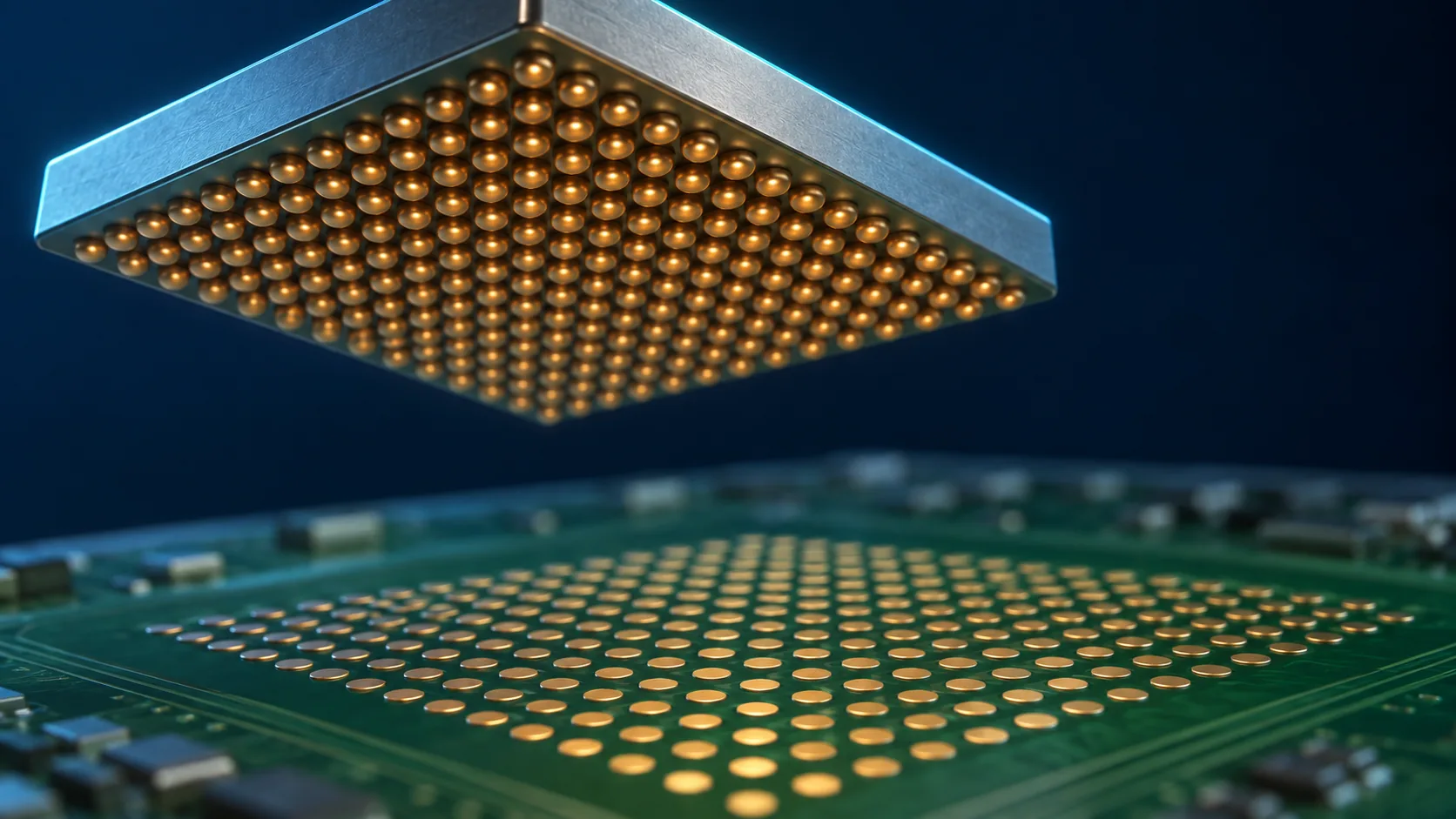
Lay the die face up and run thin wires out from its edge. That was wire bonding. Flip chip turns the die over and presses its whole face onto the substrate. The move itself is simple, yet it cut the connection length to a tenth or less, moved the heat exit to the opposite side, and replaced the entire materials set.
- What flip chip is (the short version)
- What changed — 0.1 mm against 1 to 5 mm
- Three shapes the package can take
- A materials engineer's view (1): pull out one Ni layer and the pitch tightens
- A materials engineer's view (2): turn the die over and the heat leaves the other side
- What is still hard
- Glossary / Primary sources / Claim-to-source audit
Sourced = a value stated in published material from a research institute or manufacturer (link given)
Our calculation = a figure this article derived, with the assumptions spelled out
Not yet confirmed = research-stage work with no confirmed production record
Anything beyond that — structural framing, or a reading of what it means for materials design — is marked as Commentary.
1. What flip chip is (the short version)
Flip chip means turning the die over so that the circuit side faces down, and pressing it straight onto the substrate.
- Wire bond: circuit side up, with thin wires running from edge pads across to the substrate
- Flip chip: circuit side down, with bumps spread across the face carrying every connection
- What it takes: bumps on the die (the Bump article), a joining step (the Bonding article), and a resin to fill the gap (the Underfill article)
Amkor states that it has offered flip chip in package (FCiP) technology since 1999Sourced.
2. What changed — 0.1 mm against 1 to 5 mm
While setting out the benefits of flip chip, Amkor gives one decisive number. The connection becomes "much shorter in length (0.1 mm vs. 1–5 mm)"Sourced.
Taking Amkor's figures, the ratio of connection lengths works out as followsOur calculation.
- 0.1 mm against a 1 mm wire is one tenth
- 0.1 mm against a 5 mm wire is one fiftieth
Supply noise is given by V = L × di/dt. If L drops by a factor of 10 to 50, the noise produced by the same current swing drops by the same order.
Assumption: a simplification in which inductance is proportional to length. In practice it also depends on conductor cross-section, neighbouring lines and the return-current path.
On the same page Amkor lists further benefitsSourced.
- "power can be brought directly into the core of the die"
- "entire surface of the die can be used for interconnect"
- "die to package edge requirements…can be reduced"
- "size of the die can be reduced"
Of the four, the heaviest in materials terms is "power can be brought directly into the core of the die"Sourced.
With wire bonding, power also enters from the edge. To reach the middle of the die it has to be routed a long way through the on-chip wiring. Voltage drops along the way, and the metal heats. With flip chip you put a bump directly above the middle and feed the power in from straight underneath.
That also means the boundary between chip design and packaging has moved. The power-delivery discussion in the Chiplet and Interposer articles only holds together because flip chip is assumed underneath it (commentary by this article).
3. Three shapes the package can take
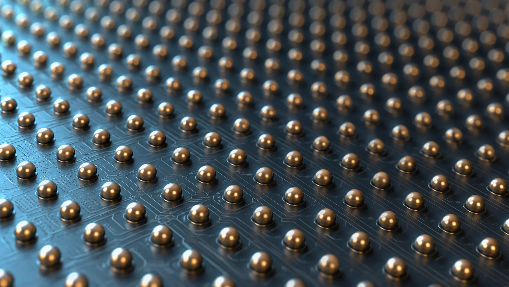
Once the die is face down on the substrate, what you put above it decides the shape of the product. Shinko Electric Industries' product line gives three representative answers.
The applications differ. Bare die goes into mobile application processors, image processors and high-speed communication packages (antennas)Sourced. The heat-spreader type goes into automotive navigation processors, image processors, SSD controller ICs and server processorsSourced.
4. A materials engineer's view (1): pull out one Ni layer and the pitch tightens
How fine flip chip can go is decided by how tightly the bump pitch can be packed. Amkor publishes "Bump pitches down to 50 µm in-line and 30/60 µm staggered" for fcCSPSourced, and "down to 30 µm in-line and 30/60 µm staggered" for copper pillarSourced.
Shinko Electric Industries says it has developed a next-generation bump structure with a 30 µm pitch and a 20 µm pad diameterSourced. And the move they made to get there is the interesting part.
As the Bump article showed, Ni is the stop layer inserted between solder and copper. It keeps Sn from eating into the copper. Ni is there for a reason.
Shinko Electric Industries nonetheless chose to take that Ni out. The reason is lateral dimension. Plating grows sideways as well as upward, so every extra layer eats into the distance to the next bump.
What is happening here is a change of direction in materials design.
- Until now: add a layer to supply the function you lack
- Further down the scaling road: look for combinations that still work with fewer layers
When the company writes that the result gives "good plating deposition and mounting reliability", it means they confirmed that dropping the Ni was safeSourced. Just as with the move to fluxless joining in the Bonding article, scaling is not only about adding usable materials; it also pushes towards finding materials you can do without (commentary by this article).
5. A materials engineer's view (2): turn the die over and the heat leaves the other side
With wire bonding the circuit side of the die faces up, which means the heat-generating face points upward and is covered in resin. The heat has nowhere to go but down into the substrate.
Flip chip reverses that. The circuit side faces down and the back of the silicon faces up. Shinko Electric Industries describes its heat-spreader flip chip package as a structure in which heat passes directly from the back of the IC chip, through a TIM (thermal interface material), into the heat spreaderSourced.
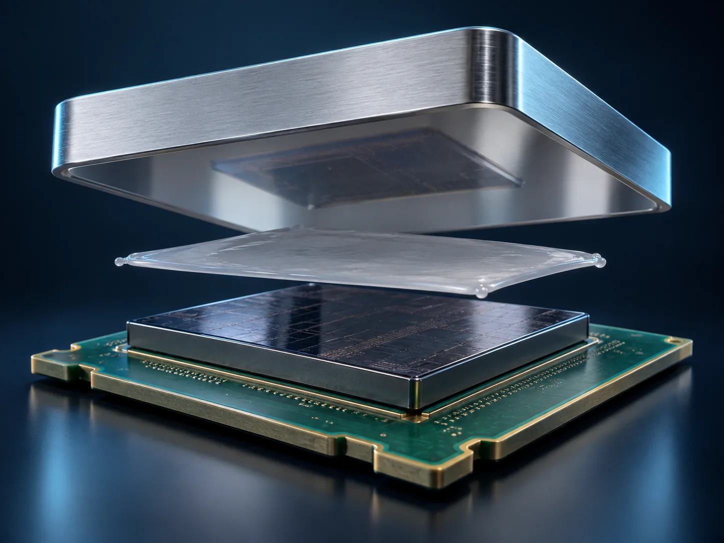
Once the die is flipped, the bare back of the silicon faces upward. Silicon conducts heat well. So lay a metal lid on top and the heat should get out — in principle.
In practice, stacking silicon and metal together does not conduct heat. Under a microscope both surfaces are rough, and they touch only at points. Air fills what is left, and air is an insulator.
What fills that gap is a TIM (thermal interface material): a material whose purpose is not adhesion but driving the air out of the interface. It is exactly the thinking behind the probe-needle contact in the Test article and the load that flattens the roughness in the Bonding article. The question of how to build an interface reappears in the thermal world (commentary by this article).
Shinko Electric Industries also says it uses its own lead frame as the heat spreader and fills the area around the IC chip with mould resin, which keeps warpage low even with a thin substrateSourced. The lid that removes the heat doubles as a structural member that holds the warpage down (commentary by this article).
6. What is still hard
(1) The moment you flip it, you can no longer see inside
With wire bonding the joints are visible from above. One wire off its pad and you can see it. With flip chip, the joints are hidden underneath the die. Visual inspection is out, and you fall back on X-ray or electrical measurement (commentary by this article).
And as the Underfill article showed, that gap is then filled with resin. An unfilled region or a void is invisible from outside.
(2) Thin it down and it becomes unhandleable
Shinko Electric Industries says its bare die product can mount IC chips thinned to 70 µm or less, and that this makes a package-on-package (PoP) stack possibleSourced.
The thinner it is, the better it stacks. But the thinner it is, the more easily it cracks and warps. That problem runs straight into the thinning issues covered in the Stacking article.
(3) Tighten the pitch and the material choices shrink
As section 4 showed, at a 30 µm pitch a single Ni layer is in the waySourced. The intermetallic volume fraction discussed in the Bump article is a constraint pointing the same way. The finer it gets, the fewer layers you are allowed and the less thickness you are permitted (commentary by this article).
Flip chip is a single move: turn the die over. That one move changed all of the following.
- Electrical: connection length falls from 1 to 5 mm down to 0.1 mm, and power can be fed straight into the core of the die
- Pads: the whole face is available, not just the edge (the Bump article)
- Thermal: the exit moved from the substrate to the upward-facing back side, which is why a TIM is needed
- Materials: bumps, UBM, underfill, moulding compound, TIM — every one of them a new materials category
Most of the back-end materials covered in this series rest on flip chip as their premise. The decision to turn the die over redrew the map of the materials industry — which is not an overstatement (commentary by this article).
7. Glossary
- Flip chip
- A mounting method in which the die is turned over, circuit side down, and connected directly to the substrate.
- Wire bond
- A method in which the circuit side faces up and fine metal wires run from edge pads to the substrate.
- FCiP
- Flip Chip in Package. A flip chip die built into a package.
- fcCSP
- Flip Chip Chip Scale Package. A flip chip package roughly the size of the die itself.
- FC-BGA
- A flip-chip-mounted package whose external terminals form a ball grid array.
- Bump
- The connection stud formed on the die side (covered in detail in the Bump article).
- In-line
- Bumps laid out in a regular grid, one row after another.
- Staggered
- Bumps offset row by row so that the effective spacing is larger.
- Underfill
- The resin that fills the gap between die and substrate (covered in detail in the Underfill article).
- Heat spreader
- The metal lid fitted over the package to spread and remove heat.
- TIM
- Thermal Interface Material. A material that fills the gap between parts so that heat passes more easily.
- PoP
- Package on Package. A structure in which one package is stacked on another.
- Inductance
- The property that opposes a change in current. The longer the wiring, the larger it gets.
- Electroless plating
- Plating that deposits metal without an external power supply.
- Lead frame
- A metal frame. Here it is used as the material of the heat spreader.
8. Primary sources
- Amkor "Flip Chip Packaging" — amkor.com
- Amkor "fcCSP (Flip Chip CSP)" — amkor.com
- Shinko Electric Industries "Fine-pitch flip chip bump technology" (Japanese-language page) — shinko.co.jp
- Shinko Electric Industries "Flip chip package with heat spreader" (Japanese-language page) — shinko.co.jp
- Shinko Electric Industries "Bare die flip chip package" (Japanese-language page) — shinko.co.jp
- Shinko Electric Industries "Mould underfill package" (Japanese-language page) — shinko.co.jp
- Amkor "Copper Pillar (Cu Pillar)" — amkor.com
9. Claim-to-source audit
| Claim in the text | Basis | Label |
|---|---|---|
| That flip chip in package (FCiP) technology has been offered since 1999. That the connection is "much shorter in length (0.1 mm vs. 1–5 mm)". The statements "power can be brought directly into the core of the die", "entire surface of the die can be used for interconnect", "die to package edge requirements…can be reduced" and "size of the die can be reduced" | Amkor "Flip Chip Packaging"[Source 1] https://amkor.com/technology/flip-chip/ | Sourced |
| That fcCSP offers "Bump pitches down to 50 µm in-line and 30/60 µm staggered"; that it "partners with all of our available bumping options (Copper Pillar, Pb-free solder, Eutectic)"; that it "Accommodates package sizes from 1×1 mm² to 25×25 mm²" | Amkor "fcCSP"[Source 2] https://amkor.com/packaging/laminate/fccsp/ | Sourced |
| That a next-generation bump structure with a 30 µm pitch and a 20 µm pad diameter has been developed; that an Ni/Pd/Au plating process is used; and the statement that applying electroless Pd/Au plating directly onto the Cu bump gives good plating deposition and mounting reliability, and that because there is no Ni layer a narrower pitch is achievable than with the conventional structure | Shinko Electric Industries "Fine-pitch flip chip bump technology"[Source 3] https://www.shinko.co.jp/rd/rd/ay/fc-bump.php | Sourced |
| That heat passes directly from the back of the IC chip, through a TIM (thermal interface material), into the heat spreader; that the company's own lead frame is used as the heat spreader; that filling the area around the IC chip with mould resin keeps warpage low even with a thin substrate; that 4-to-6-layer substrates with a 200 µm core are also supported; and that the applications include automotive navigation processors, image processors, SSD controller ICs and server processors | Shinko Electric Industries "Flip chip package with heat spreader"[Source 4] https://www.shinko.co.jp/product/package/assembly/hs-fc.php | Sourced |
| That the bare die flip chip package is a semiconductor package in which an IC chip is flip-chip mounted on an organic substrate and the joints are sealed with underfill resin; that IC chips thinned to 70 µm or less can be mounted and IC pad pitches of 45 µm or less are supported; that mounting a thinly ground IC chip makes a package-on-package (PoP) stack possible; and that the applications include mobile application processors, image processors and high-speed communication packages (antennas) | Shinko Electric Industries "Bare die flip chip package"[Source 5] https://www.shinko.co.jp/product/package/assembly/bare-die.php | Sourced |
| That MUF performs moulding and gap filling in a single step, so that the resin dispensing area needed with a liquid underfill becomes unnecessary and the package area can be reduced; and that both solder bumps and Cu pillars are supported | Shinko Electric Industries "Mould underfill package"[Source 6] https://www.shinko.co.jp/product/package/assembly/muf.php | Sourced |
| That copper pillar is "Fine pitch capable down to 30 µm in-line and 30/60 µm staggered" | Amkor "Copper Pillar"[Source 7] https://amkor.com/technology/copper-pillar/ | Sourced |
| The ratio of connection lengths (one tenth against 1 mm, one fiftieth against 5 mm), and the statement that inductance and supply noise (V = L × di/dt) fall by the same order | Our calculation. A simplification in which inductance is proportional to length, excluding the effect of cross-sectional shape, neighbouring lines and the return path. The underlying lengths come from Source 1[Source 1] https://amkor.com/technology/flip-chip/ | Our calculation |
| That among the values placed side by side in Fig. 6, in-line and staggered arrangements are measured differently and cannot be compared directly | Our note. The figures themselves come from Sources 1, 2, 3 and 7 | Commentary |
| The framing that wire bonding can only send heat down into the substrate; the heat directions drawn as arrows in Fig. 8; the explanation that stacking silicon and metal leaves air at the interface so heat does not pass, and the reading that a TIM is a material for driving air out rather than for adhesion; the observation that the heat-removing lid doubles as a structural member holding warpage down; the way Fig. 5 draws the Ni layer as something that costs lateral dimension; the framing of a turn from adding layers to removing them; the observation that flipping the die hides the joints from view; and the framing that much of the back-end materials set in this series rests on flip chip as its premise | Commentary by this article, built on published material. These are not positions stated by the companies | Commentary |
| That the cross-sections in Figs. 1, 4, 5 and 8 are explanatory drawings rather than real observed images | Our note | Commentary |
Last updated 20 September 2026. Sources are limited to primary material (official technology and product pages published by package manufacturers). Because the article includes structural framing and readings of the materials design, those parts are marked as Commentary and kept distinct from sourced fact. All figures are explanatory concept graphics. Visual-overview figures are shown as AI-generated conceptual images, matching the Japanese edition. Vector drawings are retained where they carry quantitative values or precision-critical technical labels. AI-generated images do not depict real equipment, products, facilities, dimensions or exact cross-sections; replaced source SVG overview drawings remain in the HTML but are hidden.