TECHNOLOGY EXPLAINER
What Hybrid Bonding Is
— throw away the solder, join copper straight to copper
Chip joints have leaned on solder for the best part of a century. Hybrid bonding drops that assumption and joins copper and dielectric directly, atom to atom. Written for readers meeting the technology for the first time, and for the materials engineers who have to make it work.
- What hybrid bonding is (the short version)
- Why it was needed — where solder runs out
- How the joint is actually made (four steps)
- Why a few nanometres decide everything
- A materials engineer's view: SiCN, CMP, cleaning, particles
- W2W and D2W — two ways of doing it
- Real products (it is already in your phone)
- What is still hard
- What comes next
- Glossary / Primary sources / Claim-to-source audit
Sourced = a value stated in published material from a research institute or manufacturer (link given)
Our calculation = a figure this article derived, with the assumptions spelled out
Not yet confirmed = research-stage work with no confirmed production record
1. What hybrid bonding is (the short version)
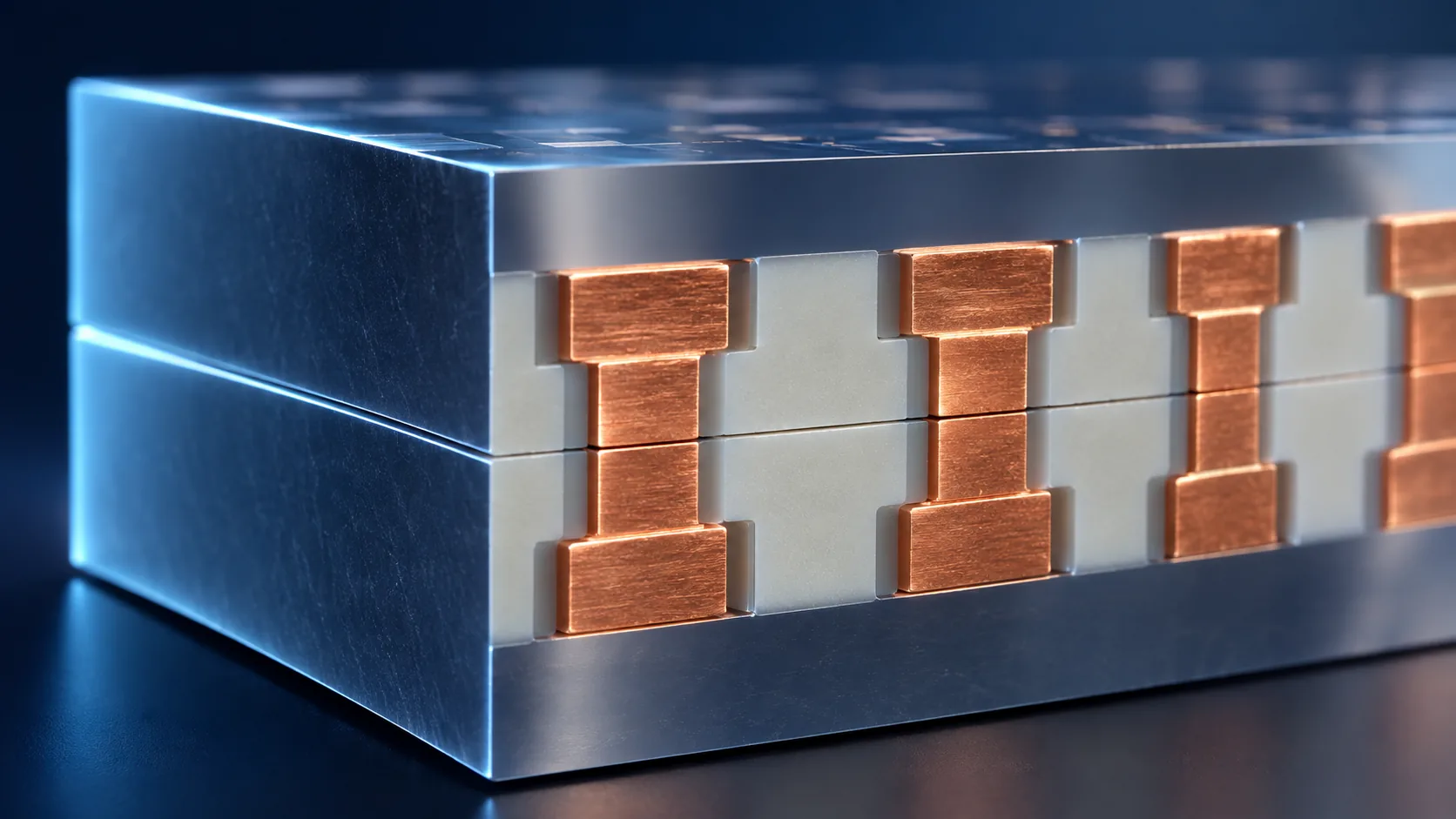
Hybrid bonding is a way of joining two chips that uses no solder bumps at all: the copper electrodes and the insulating film are bonded directly, both at the same time.
- No solder: nothing is melted. Two flat surfaces are brought into contact and bond at the atomic level
- Two materials bonded at once: dielectric to dielectric, and copper to copper, in a single process
- Hence "hybrid": the name simply records that two bonds of very different character are combined
The payoff shows up directly in interconnect density. For its 3D V-Cache technology, AMD states that the bumpless, copper-to-copper hybrid bonded construction delivers more than 200 times the interconnect density of 2D chiplets on a package, and more than 15 times that of other 3D technologies that use solder bumps, along with more than three times the energy efficiency per connectionSourced (AMD).
2. Why it was needed — where solder runs out
Solder cannot be made fine
A solder bump is joined by melting it. Once molten it pulls itself round under surface tension and spreads sideways. Make the bumps narrower and the spacing tighter, and neighbouring bumps eventually touch and short. That is a physical floor, not an engineering inconvenience.
imec places solder-based bonding at a pitch of 5–10 µm and wafer-to-wafer hybrid bonding below 1 µmSourced (imec). Close to an order of magnitude separates the two.
Resin stops flowing into the gap
Bonding with solder bumps always leaves a gap between the dies, and that gap has to be filled with underfill resin to relieve stress and protect the bumps. The finer the pitch, the narrower the gap, until capillary action can no longer draw the resin in. Any void left behind is a break in the thermal path and a starting point for delamination.
The bump itself is a resistor
Electrically and thermally, a solder bump is dead length. Once a package carries tens of thousands of connections, the resistance and parasitic capacitance of each one add up and push power consumption higher. AMD's claim of more than three times the energy efficiency per connection is what you get when that length is removed altogether.
If solder cannot be made fine enough, stop melting anything. Take the solder away and the spreading, the gap and the parasitic resistance all disappear together. What the process demands in return is a surface flat and clean enough to stick without melting. Every difficulty in hybrid bonding traces back to that one requirement.
3. How the joint is actually made (four steps)
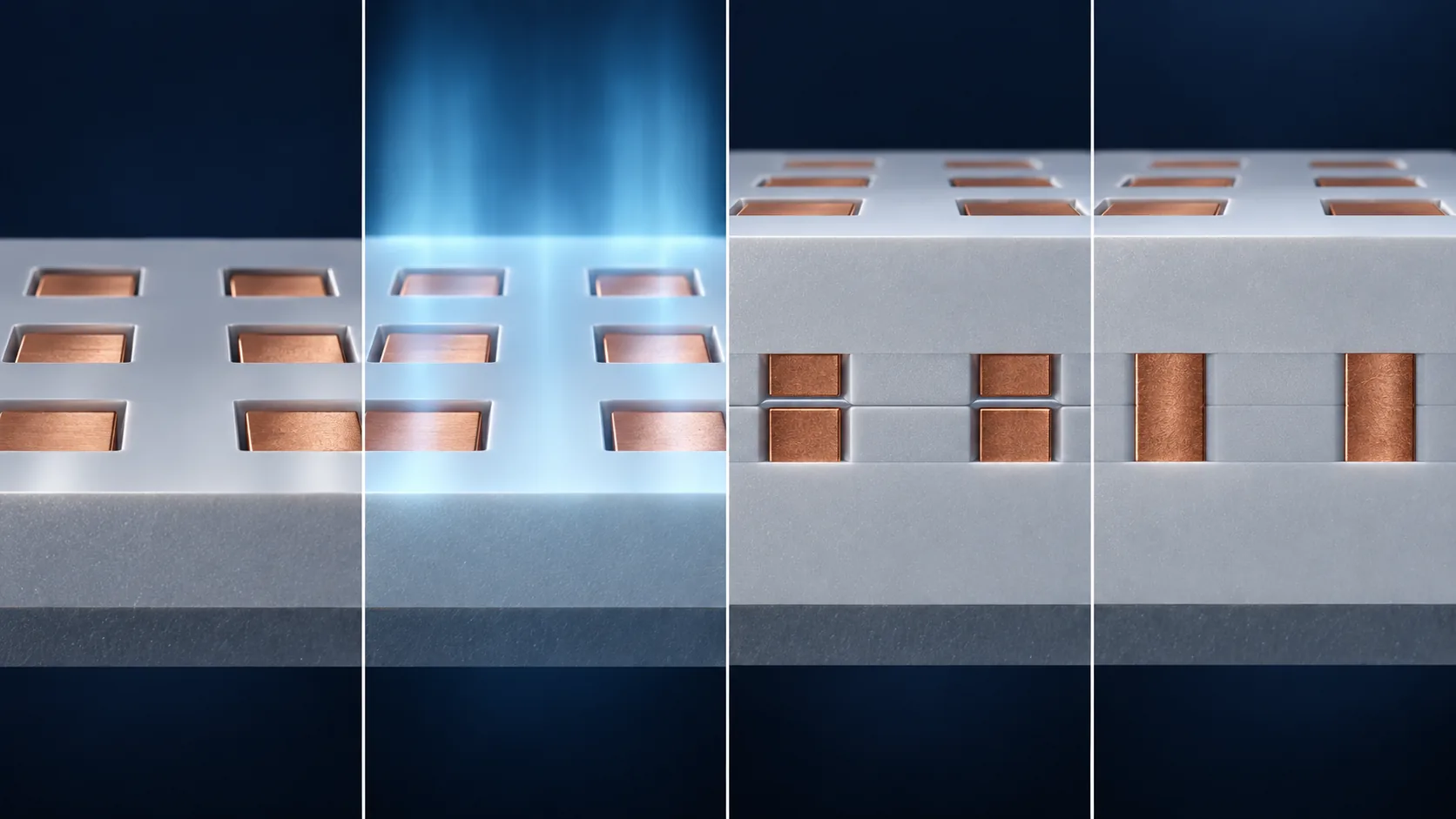
The counter-intuitive part: the copper is deliberately polished low
Step 1 is the one that feels wrong. The copper electrodes are polished by CMP until they sit a few nanometres below the bonding surface. The very electrodes that have to connect are deliberately recessed.
imec gives a copper pad recess below 2.5 nm as a condition for a good bond, and explains that it optimised the CMP process on the Cu/SiCN surface to achieve high uniformity across the whole wafer in order to get thereSourced.
In step 3, the room-temperature bond, only the dielectrics join; the copper has still not made contact. It is the anneal in step 4 that finishes the job: the copper expands thermally, closes the few-nanometre gap itself, and bonds copper to copper. Thermal expansion of metal, normally treated as a nuisance, is designed in here as the driving force of the bond — which is the neatest idea in the whole process.
4. Why a few nanometres decide everything
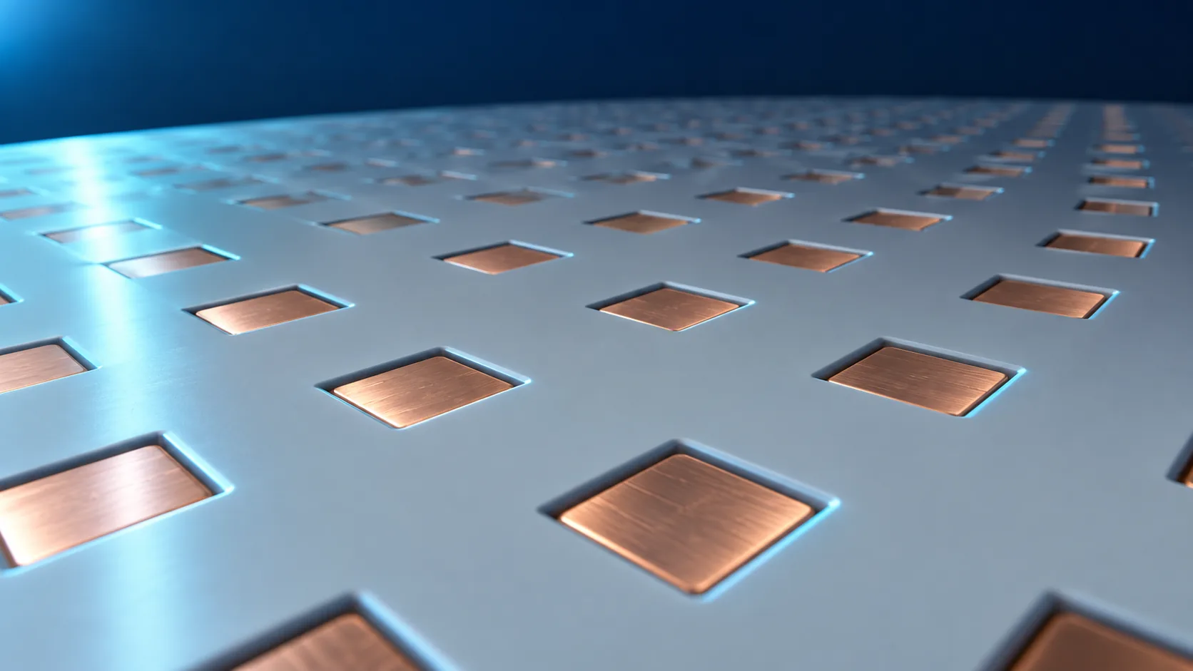
The tolerance on the recess is, on its own, a fair measure of how hard this technology is.
A 300 mm wafer has an area of roughly 706 cm²Our calculation. Across all of it, the copper height has to be held inside a window a few nanometres wide. Picture levelling an area the size of a city to within a millimetre everywhere and the difficulty starts to come across.
To achieve that control, imec explains that it used an advanced CMP process together with dummy pads in the layout design, giving precise control of copper pad height and surface topography across the full waferSourced. Patterns that carry no signal are put there for one reason: to stop the polish rate varying from place to place.
5. A materials engineer's view: SiCN, CMP, cleaning, particles
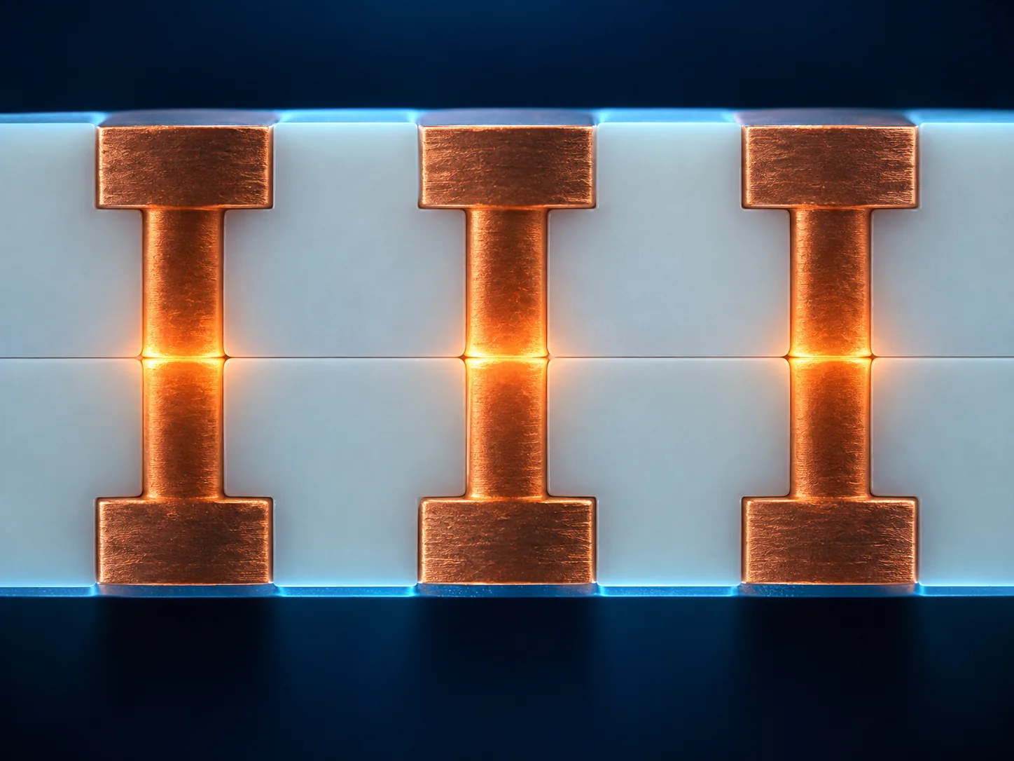
This, for our money, is the most interesting part of the story. Hybrid bonding removes a bonding material and swaps in another one at the same time.
(1) Organic materials leave, inorganic materials take over
Drop the solder and the flux goes with it, and so does the underfill resin and everything done to protect it. What decides success instead is the inorganic materials that form the bonding surface, and the chemistries that polish and clean them.
| Solder bump bonding | Hybrid bonding | |
|---|---|---|
| Bonding material | Solder alloy, with organic flux | Copper plus dielectric (SiCN or SiO2) |
| Filling the gap | Underfill resin | There is no gap to fill |
| What drives the bond | Melting under heat | Surface bonding plus thermal expansion of copper |
| The critical step | Reflow and resin fill | CMP, cleaning, cleanliness control |
| Where the materials business sits | Solder, resins, fillers | CMP slurries, cleaning chemistries, deposition materials |
The left-hand column is the territory covered in our HBM and chiplet articles. A change of generation in bonding technology is also a change in the cast of the materials industry.
(2) SiCN rather than SiO2 — the material choice sets the pitch
For the dielectric at the bonding surface, the direction of travel is away from conventional SiO2 and towards SiCN, silicon carbonitride. imec proposes SiCN as the dielectric for fine pitches and gives these reasonsSourced.
1. Higher bonding energy than an SiO2 surface (SiCN-to-SiCN bond strength is well above SiO2-to-SiO2)
2. It acts as a diffusion barrier for copper
3. As a wafer passivation layer it blocks gas diffusion
4. The result is a thermally more stable bonding interface
imec also reports that high bond strength is reached at an anneal temperature of 250 °C, and does not degrade above it. The lower the bonding temperature, the less thermal load on the devices and wiring underneath. Choosing the dielectric is what sets both the pitch you can reach and the thermal budget you have to spend — a textbook case of materials being the rate-limiting factor.
(3) One particle ruins a wide area
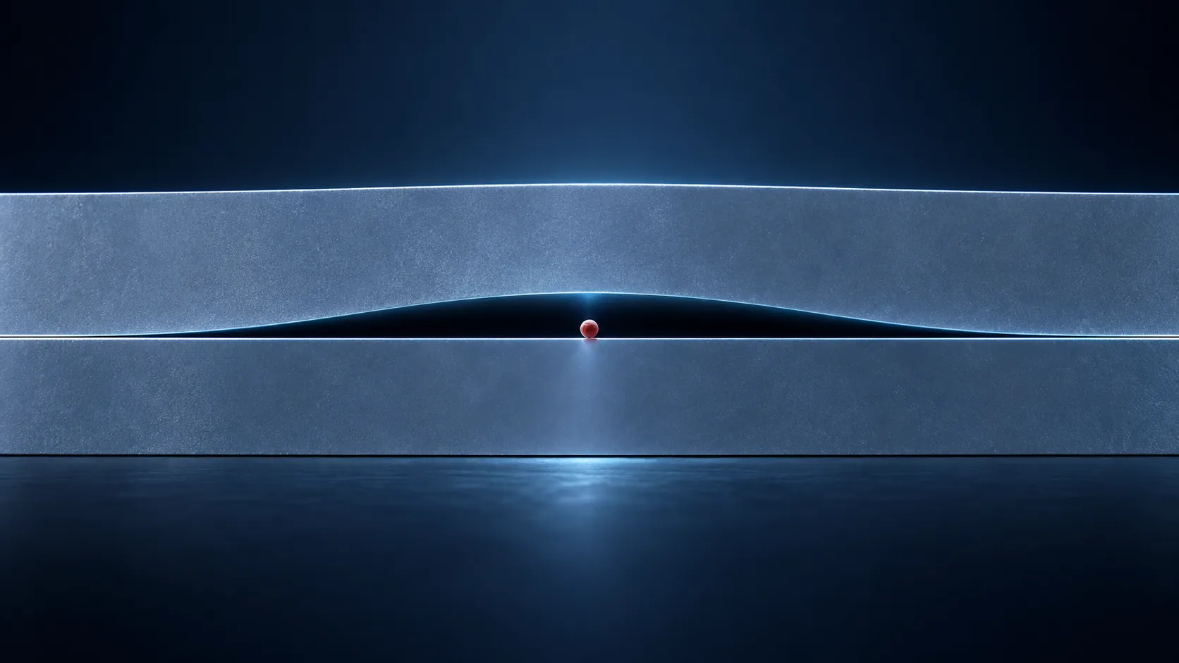
In solder bonding, molten solder will sometimes simply push a small piece of debris aside. In hybrid bonding, a single particle on the bonding surface lifts everything around it, leaving a wide unbonded region.
That is why imec adopted plasma dicing for separating the dies: to get "high-quality singulation without generating particles and without affecting the Cu/SiCN surface", with the emphasis on "maintaining ultra-clean surfaces throughout processing, singulation and pick-and-place"Sourced.
Conventional dicing with a mechanical blade inevitably produces swarf. A quality requirement at the bond reaches back several steps and changes how the wafer is cut. That is one reason hybrid bonding is not a drop-in change.
6. W2W and D2W — two ways of doing it
Hybrid bonding comes in two broad flavours.
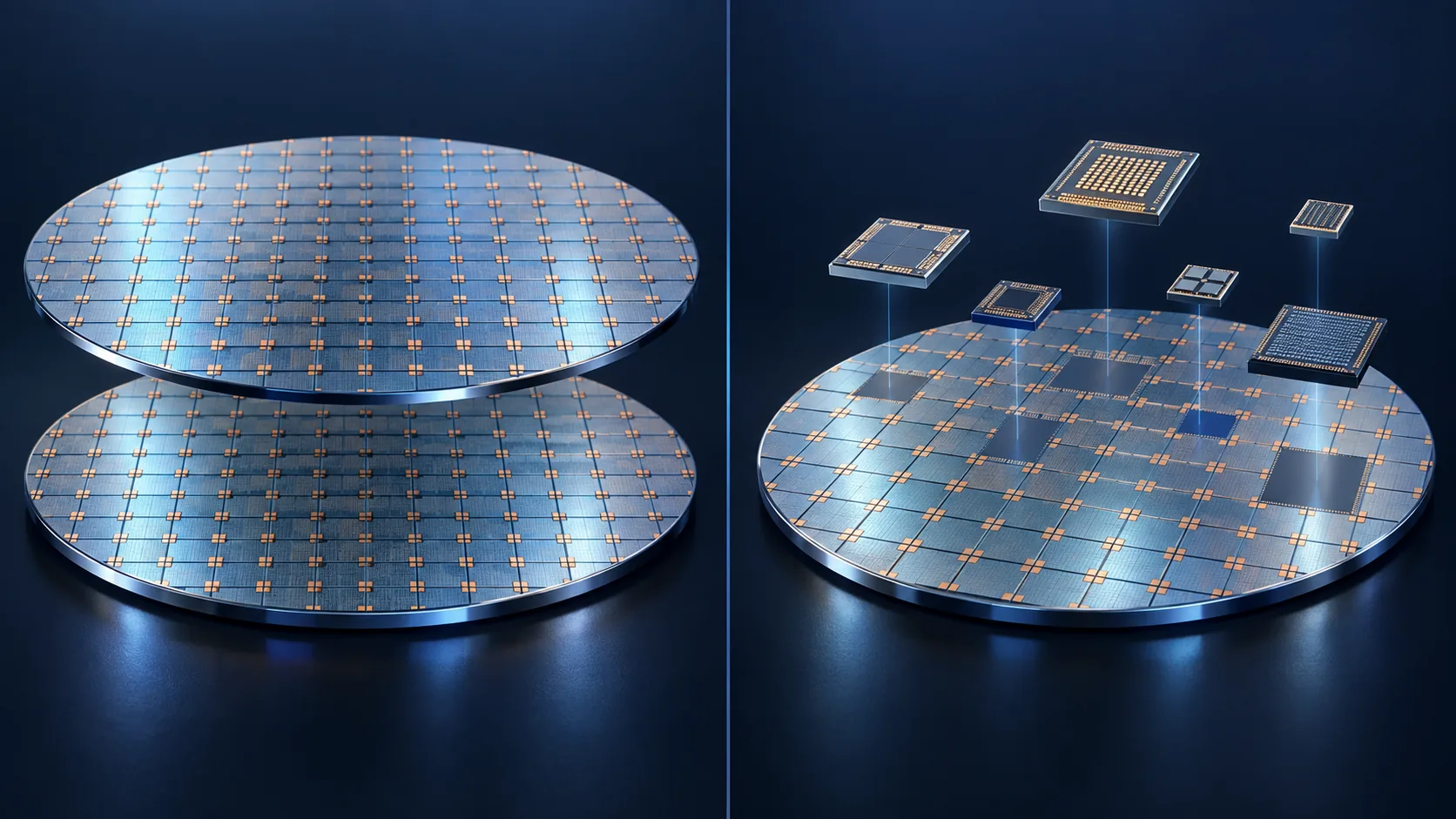
| W2W (wafer to wafer) | D2W (die to wafer) | |
|---|---|---|
| How it works | Two 300 mm wafers are bonded together in one go | Individual singulated dies are placed on a wafer and bonded |
| Pitch demonstrated by imec | 200 nm | 2 µm |
| Alignment achieved (same work) | Post-bond overlay below 40 nm across 100% of a 300 mm wafer | Die-to-wafer overlay error below 350 nm |
| Strengths | Alignment is easier, so the finest pitches are within reach | Dies of different sizes can be mixed, and only known-good dies need be placed |
| Weaknesses | Upper and lower dies must be the same size, and there is no way to sort out bad dies | Particle control during singulation and placement accuracy are the open problems |
All of the above is Sourced from imec publications. The 200 nm W2W result is the imec and EV Group announcement of May 2026; the 2 µm D2W result is imec's announcement of May 2024.
Seen from the chiplet side, D2W matters more: it is what lets you combine dies of different sizes made on different processes, and place only the good ones. That practical point is why imec frames its 2 µm D2W result as "bridging the gap between solder bonding at 5–10 µm and W2W hybrid bonding below 1 µm"Sourced.
7. Real products (it is already in your phone)
Describing the evolution of its stacked CMOS image sensors, Sony Semiconductor Solutions states that in 2015 it achieved the world's first Cu-Cu (copper-to-copper) connection, enabling smaller size, higher performance and better productivitySourced (Sony Semiconductor Solutions). Hybrid bonding reached volume production in phone cameras, well before AI accelerators or leading-edge CPUs.
| When | Product or technology | What has been published |
|---|---|---|
| 2015 | Sony stacked CMOS image sensor | World's first Cu-Cu connection. Smaller size, higher performance, better productivity |
| — | AMD 3D V-Cache | Bumpless chip-on-wafer construction using copper-to-copper hybrid bonding. More than 200 times the interconnect density of 2D, more than 15 times that of solder-bump 3D, and more than three times the energy efficiency per connection |
| — | AMD second-generation 3D V-Cache | The cache die moves below the compute cores so that the cores sit against the heatsink, inverting the earlier design. The Ryzen 7 9850X3D gains 400 MHz of boost clock over the previous generation |
| — | Intel Foveros Direct 3D | Hybrid bonding at sub-10 µm bump pitch. Up to ten times the interconnect density of conventional microbumps |
| — | TSMC SoIC | Bond pitch from below 10 µm. Supports both CoW (chip on wafer) and WoW (wafer on wafer) |
All of the above is Sourced from each company's published material.
AMD turned the stack upside down because of heat. With the hot cores underneath and the cache on top, core heat can only escape through the cache. Invert the two and the cores face the cooler directly. The result was 400 MHz more clock — a worked example of thermal design becoming the next constraint once bonding technology improves.
8. What is still hard
(1) Yield
For its 2 µm-pitch D2W demonstration, imec reports electrical yields of above 85% on Kelvin structures and above 70% on daisy chainsSourced. That is strong for a research demonstration, but still some distance from production quality.
(2) Alignment accuracy
For W2W, imec states that "overlay control below 100 nm is needed to obtain sufficient yield in volume manufacturing"Sourced. As the pitch shrinks, the permitted misalignment shrinks in proportion.
(3) Cleanliness and equipment
As section 5 argued, particle control is decisive. It is not only the bonder: CMP, cleaning, dicing and handling all have to be brought up to a new cleanliness standard, which means an existing back-end line cannot simply be repurposed. That is where the cost of entry comes from.
(4) Heat
The thinner the bond and the denser the stack, the harder it is for heat to get out. AMD inverting the stack in the second generation is one concrete answer to that problem.
9. What comes next
Finer pitch still: imec and EV Group have demonstrated W2W bonding at 200 nm pitchSourced. The UCIe specification also brings pitches below 1 µm into scope for its 3D profileSourced.
D2W in production: exploiting the combinatorial freedom of chiplets requires D2W, and imec is continuing to develop itSourced.
HBM, with its ever-growing stack height, is widely seen as a promising target for hybrid bondingNot yet confirmed. However, as of our research for this article (September 2026) we could find no official manufacturer announcement of hybrid bonding used in HBM volume production.
Trade coverage disagrees on when it will arrive. When this topic comes up, we would suggest keeping roadmap targets and production track record clearly apart.
10. Glossary
- Hybrid bonding
- Joining copper electrodes and dielectric directly and simultaneously, with no solder bumps.
- Bumpless
- A connection made without any solder bump in between.
- Dielectric bonding
- Bringing two insulating films into contact so that they bond. It proceeds even at room temperature.
- SiCN
- Silicon carbonitride. The bonding dielectric of choice for fine pitch; it also acts as a copper diffusion barrier.
- CMP
- Chemical mechanical polishing. Planarises a surface by combining chemical reaction with mechanical abrasion.
- Recess (dishing)
- How far the copper sits below the surrounding dielectric after CMP. Control to a few nanometres is required.
- Dummy pad
- A pattern that carries no signal, placed to make the CMP removal rate uniform.
- Anneal
- The heat treatment after bonding. It expands the copper and completes the metal-to-metal joint.
- Overlay
- The misalignment between upper and lower layers. The finer the pitch, the tighter the requirement.
- W2W
- Wafer-to-wafer. Bonding two wafers together.
- D2W
- Die-to-wafer. Bonding singulated dies onto a wafer.
- Plasma dicing
- Singulating a wafer with plasma rather than a blade. It produces no swarf.
- Kelvin structure
- A test structure for measuring the resistance of a connection precisely.
- Daisy chain
- A test structure wiring many connections in series, so that a single open circuit shows up.
11. Primary sources
- imec "imec demonstrates die-to-wafer hybrid bonding with Cu interconnect pad pitch of 2um", 29 May 2024 — imec-int.com
- imec "imec and EV Group demonstrate wafer-to-wafer hybrid bonding with 200nm interconnect pitch", 28 May 2026 — imec-int.com
- imec "Wafer-to-wafer hybrid bonding: pushing the boundaries to 400nm interconnect pitch" — imec-int.com
- Sony Semiconductor Solutions "Common Technology of Image Sensors" — sony-semicon.com
- AMD "AMD 3D V-Cache Technology" — amd.com
- Intel "Advanced Packaging Innovations" — intel.com
- Intel "Foveros Direct 3D Technology Brief" — intel.com (PDF)
- TSMC "TSMC-SoIC" technology page — 3dfabric.tsmc.com
- UCIe Consortium "Specifications" — uciexpress.org
12. Claim-to-source audit
| Claim in the text | Basis | Label |
|---|---|---|
| Solder bonding is placed at 5–10 µm pitch and W2W hybrid bonding below 1 µm | imec press release, 29 May 2024[Source 1] https://www.imec-int.com/en/press/imec-demonstrates-die-wafer-hybrid-bonding-cu-interconnect-pad-pitch-2mm | Sourced |
| D2W demonstrated at 2 µm pitch; Cu recess below 2.5 nm; SiCN used; die-to-wafer overlay error below 350 nm; plasma dicing adopted; ultra-clean surfaces maintained throughout | imec press release, 29 May 2024[Source 1] https://www.imec-int.com/en/press/imec-demonstrates-die-wafer-hybrid-bonding-cu-interconnect-pad-pitch-2mm | Sourced |
| Electrical yield of the D2W demonstration: above 85% on Kelvin structures, above 70% on daisy chains | imec press release, 29 May 2024[Source 1] https://www.imec-int.com/en/press/imec-demonstrates-die-wafer-hybrid-bonding-cu-interconnect-pad-pitch-2mm | Sourced |
| W2W demonstrated at 200 nm pitch, with post-bond overlay below 40 nm across 100% of a 300 mm wafer | imec and EV Group announcement, 28 May 2026[Source 2] https://www.imec-int.com/en/press/imec-and-ev-group-demonstrate-wafer-wafer-hybrid-bonding-200nm-interconnect-pitch-and-record | Sourced |
| SiCN has higher bonding energy than SiO2, acts as a Cu diffusion barrier and a gas diffusion block, and is thermally stable; high bond strength is reached at a 250 °C anneal and does not degrade above it | imec technical article (400 nm pitch)[Source 3] https://www.imec-int.com/en/articles/wafer-wafer-hybrid-bonding-pushing-boundaries-400nm-interconnect-pitch | Sourced |
| The Cu connection pitch used in production is about 1 µm, and volume manufacturing needs overlay control below 100 nm | imec technical article (400 nm pitch)[Source 3] https://www.imec-int.com/en/articles/wafer-wafer-hybrid-bonding-pushing-boundaries-400nm-interconnect-pitch | Sourced |
| CMP combined with dummy pads controls copper pad height and surface topography across the full wafer | imec published material[Source 3] https://www.imec-int.com/en/articles/wafer-wafer-hybrid-bonding-pushing-boundaries-400nm-interconnect-pitch | Sourced |
| Sony achieved the world's first Cu-Cu connection in 2015 (stacked CMOS image sensor) | Sony Semiconductor Solutions technology page[Source 4] https://www.sony-semicon.com/en/technology/is/index.html | Sourced |
| AMD 3D V-Cache: more than 200 times the interconnect density of 2D and more than 15 times that of solder-bump 3D, more than three times the energy efficiency per connection, bumpless chip-on-wafer | AMD product technology page[Source 5] https://www.amd.com/en/products/processors/technologies/3d-v-cache.html | Sourced |
| The second-generation 3D V-Cache moves the cache below so the cores face the cooler; the Ryzen 7 9850X3D gains 400 MHz of boost clock | AMD product technology page[Source 5] https://www.amd.com/en/products/processors/technologies/3d-v-cache.html | Sourced |
| Foveros Direct 3D uses sub-10 µm pitch and reaches up to ten times the interconnect density of conventional microbumps | Intel published material[Source 6] https://www.intel.com/content/www/us/en/foundry/packaging.html | Sourced |
| TSMC SoIC bond pitch starts below 10 µm and supports both CoW and WoW | TSMC SoIC technology page[Source 8] https://3dfabric.tsmc.com/english/dedicatedFoundry/technology/SoIC.htm | Sourced |
| A 300 mm wafer has an area of about 706 cm² | Our calculation: π × (15 cm)² | Our calculation |
| That molten solder spreads and so sets a floor on pitch, that resin stops flowing into the gap, and that the bump is dead length electrically and thermally | Commentary based on the underlying physics. No specific numerical claim is made | Commentary |
| Hybrid bonding applied to HBM volume production | No official manufacturer announcement found as of the research for this article | Not yet confirmed |
Last updated 20 September 2026. Sources are limited to primary material (published documents from research institutes, and official announcements and technology pages from manufacturers). All figures are explanatory concept graphics. Visual-overview figures are shown as AI-generated conceptual images, matching the Japanese edition. Vector drawings are retained where they carry quantitative values or precision-critical technical labels. AI-generated images do not depict real equipment, products, facilities, dimensions or exact cross-sections; replaced source SVG overview drawings remain in the HTML but are hidden.