TECHNOLOGY EXPLAINER
What Silicon Photonics Is
— building optical parts in a semiconductor fab
Optical components lived for decades in a world of compound semiconductors and glass. Silicon photonics moves them onto a silicon production line. Waveguides, modulators, photodetectors — all of them made with CMOS process steps. With one exception: silicon cannot emit light — and the hardest part of all is getting light in and out.
- What silicon photonics is (the short version)
- Why handle light in silicon at all
- What gets built — the four components
- A materials engineer's view 1: light travels well, it just hates doorways
- A materials engineer's view 2: what silicon cannot do
- What is still hard
- Glossary / Primary sources / Claim-to-source audit
Sourced = a value stated in published material from a research institute or manufacturer (link given)
Our calculation = a figure this article derived, with the assumptions spelled out
Not yet confirmed = research-stage work with no confirmed production record
Anything that is our own structural reading or materials-design interpretation is marked separately as Commentary.
1. What silicon photonics is (the short version)
Silicon photonics means using the silicon semiconductor process to build circuits that handle light.
imec puts the advantage this way: "With this scalable technology, compact and low-power transceivers can be implemented at low cost and high volume, by leveraging existing CMOS fabrication infrastructure." Sourced
- What gets built: waveguides (the path for light), modulators (putting an electrical signal onto light), photodetectors (turning light back into current), couplers (joining to the fibre)
- What it is built on: SOI wafers. imec works on 200 mm and 300 mm SOI wafersSourced
- What it cannot do: emit light. Silicon does not make a laser
Two earlier articles already deal with light. This one takes the device and materials side.
- Why light comes into the package at all (the system argument) → the Co-Packaged Optics article
- How the electronic die and the photonic die get stacked (the assembly) → the Heterogeneous Integration article (TSMC COUPE)
- The optical components themselves, and their materials → this article
2. Why handle light in silicon at all
Optical communication parts were originally made from compound semiconductors such as InP (indium phosphide) and glass. The reason for moving them to silicon is not performance. It is manufacturing infrastructure.
Silicon is not a specially good material for handling light. It carries one decisive weakness: it cannot emit light (section 5).
Silicon won anyway, because the production lines already exist, in enormous quantity, all over the world. When imec writes "leveraging existing CMOS fabrication infrastructure", that is exactly what it meansSourced.
By the usual logic of materials development this is backwards. Normally you go looking for the material best suited to the job. Here, the job was fitted to the material that can be manufactured.
It is the mirror image of the argument in the glass substrate article of this series — glass is the better material, but getting it onto the silicon and resin production infrastructure is the hard part (Commentary).
3. What gets built — the four components
Silicon photonics builds four broad kinds of component. For modulators, imec says it has developed three variants — "Si ring modulators", "Si Mach-Zehnder modulators" and "GeSi based electro-absorption modulators" — and that photodetectors are co-integrated with CMOS metallisation through "selective-area growth of Ge"Sourced.

4. A materials engineer's view 1: light travels well, it just hates doorways
Look at the numbers and something unexpected comes out. Light is remarkably good at covering distance. What is hard is the moment it enters, and the moment it leaves.
TSMC Research has published the following measured values for its EPIC-BOE optical engine technologySourced.
| Item | Published value | What it means |
|---|---|---|
| Waveguide propagation loss | < 0.01 dB/cm | Travel a whole centimetre and lose under 1% |
| Loss per 90-degree bend | < 0.001 dB/turn | Turn a right angle and lose almost nothing |
| Layer-to-layer transition loss | 0.015 dB | The cost of moving between waveguide layers |
| Fibre coupling loss | 0.08 dB | One single joint between fibre and chip |
| Polarisation handling element (PBSR) | loss < 0.3 dB, extinction ratio > 23 dB | Over 1260 to 1360 nm, for both TE and TM modes |
All values follow TSMC Research, "EPIC-BOE" (2024) [Source 2]. The right-hand column is our own explanation.
Divide the published values into each otherOur calculation.
- The waveguide costs 0.01 dB/cm. A fibre coupling costs 0.08 dB. → one coupling = 8 cm of waveguide
- A 90-degree bend costs 0.001 dB. → one bend = 1 mm of waveguide. One coupling is worth 80 bends
- Run the waveguide a full 1 m (100 cm) and you are still under 1 dB
Assumptions: these are plain multiplications and divisions of published per-unit values. In reality the coupling depends on its design, on process variation, on temperature and on polarisation state.
The reading is unambiguous. Routing light around inside the chip costs almost nothing. The cost is concentrated at a single point: where the chip meets the fibre (Commentary).
The Co-Packaged Optics article noted that Resonac showed, as a reference exhibit, an adhesive for bonding the PIC to the FAUSourced. Why would an adhesive be worth a booth at a technology show? The numbers in this section are the answer.
Optical loss is concentrated at the joint. And sitting in that joint is the adhesive layer holding the PIC and the fibre array together. Light passes straight through that layer, so what is demanded of it is not adhesion.
- Transparency: no absorption in the band in use (1260 to 1360 nm, for instance)
- Index matching: a refractive index mismatch reflects light at the interface
- Dimensional stability: if cure shrinkage or a temperature swing moves the parts, coupling loss rises
- Photostability: no degradation under continuous high-power light
TSMC's SiN fibre coupler is verified to "withstand high input laser power of > 300 mW for 3 hours without degradation"Sourced. Which is another way of saying that is how much light is concentrated at the joint (Commentary).
In from the edge, or in from the top
There are two broad ways to join a fibre to a chip. TSMC Research states the advantage of the vertical coupler as follows: "Unlike the conventional broadband solution- edge coupler (EC), this solution is immune from beachfront warpage issue when we integrate 40 to 80 fibers per row." Sourced
5. A materials engineer's view 2: what silicon cannot do
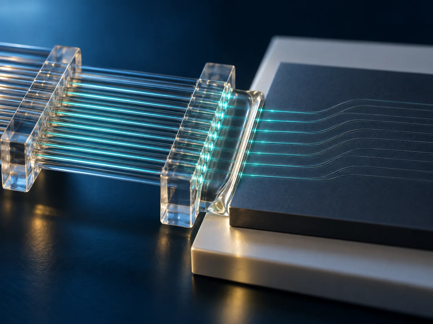
So far, what silicon can build. Now, what it cannot.
Silicon does not emit light. Because of its crystal structure, it converts electricity into light with vanishingly low efficiency. So the laser source, and only the laser source, has to come from another material — a compound semiconductor such as InP.
As the Co-Packaged Optics article described, OIF has defined ELSFP, a standard for external laser sources, which places the laser on "the front panel, the coolest section of the system" to deliver improved system reliability and hot-swappable replacementSourced.
The history of silicon photonics is partly a history of trying to make silicon lase. The configurations that actually reached production sidestep the problem rather than solve it.
- The light source is made from another material, such as InP
- And it sits outside the package, not inside the chip
- Light is piped in over fibre, and the silicon circuit only modulates and detects
In other words, silicon photonics gave up the job of making light and specialised in the job of steering it. That concession is precisely what protects its one great advantage: volume production on a CMOS line.
The design instinct this series keeps running into — do not make one thing do everything, split the work by what each part is good at, the selective use of silicon in the bridge article, the material-specific parts in the SiP article — is applied here against a hard limit of material physics (Commentary).
And then the demands on the material light passes through
AGC lists the strengths of its polymer waveguides (PWG) and glass waveguides (GWG) for optical wiring as high transmittance in the O band and C band, reflow compatibility and durability against high-power lasers, and fine patterning by photolithographySourced.
As the Co-Packaged Optics article argued, those three pull against each other. Patterning by photolithography (please react to light) and durability against high-power lasers (please do not change under light) are in direct contradiction (Commentary).
6. What is still hard
Silicon photonics is not a research-stage technology. As far back as 2018 imec wrote that with it "compact and low-power transceivers can be implemented at low cost and high volume, by leveraging existing CMOS fabrication infrastructure"Sourced. And yet the problems that remain are concentrated on the materials side.
Hard problem 1: coupling decides the yield
As section 4 showed, the loss is concentrated at the joints. And there are as many joints as there are fibres. When TSMC speaks of 40 to 80 fibres per row, it means a single optical engine carries dozens of themSourced.
The yield multiplication set out in the Co-Packaged Optics article — with a per-joint success rate of p across n joints the whole comes to pn — applies here in exactly the same shape (Commentary). Forty fibres are aligned one by one, bonded and cured. Only when every one of them lands within the required alignment tolerance does the optical engine meet its specification.
When TSMC says of the vertical coupler that "The FAU system can then be made field serviceable", that is partly an answer to this yield problemSourced. If you join it wrong, make it possible to join it again. It points in the same direction as making the laser hot-swappable, which the Co-Packaged Optics article described (Commentary).
Hard problem 2: temperature moves the wavelength
Of the modulators imec lists, the ring modulator is a structure that resonates at a particular wavelengthSourced. That resonant wavelength is set by the refractive index and the dimensions of the ring.
Which brings up a problem every materials engineer already knows. Refractive index and dimensions both move with temperature (Commentary). An electrical circuit keeps working when its characteristics drift a little with heat. A ring modulator does not: once the resonance shifts, the light stops getting through.
So in optical engine design, the distance to the heat source (the logic die), the thermal conductivity of the encapsulant and the thermal expansion of the substrate all feed directly into optical performance. The heat-and-stress discussions running through this series turn out to be optical design discussions as well (Commentary).
Hard problem 3: made by light, yet resistant to light
The three AGC requirements mentioned in section 5 — high transmittance, photolithographic patterning, and durability against high-power lasers — point at a difficulty common to every material that light has to pass throughSourced.
"React to light, but do not degrade under light" is a demand that shows up in exactly the same shape in photoresists and in light-cured adhesives.
- Separate the exposure wavelength from the working wavelength (UV for exposure, O or C band in use)
- Destroy the photosensitive groups after cure (post-cure, post-bake)
- Keep the photosensitive component out of the optical path (core and cladding material design)
Waveguide materials for silicon photonics have to solve that design problem with the added condition of surviving reflow temperature (Commentary). The thermal constraints seen in the build-up film article and the underfill and encapsulant article arrive here at the same time as the optical constraints.
Hard problem 4: standardisation is not finished
OIF has published an Implementation Agreement for 3.2T co-packaged modules and another for the ELSFP external laser sourceSourced. The inside of the optical engine, though — waveguide material, coupling scheme, how the FAU is fixed — remains proprietary to each vendor. Which approach becomes the industry standard is not settled todayNot yet confirmed.
- Silicon photonics builds optical components on a silicon CMOS line. imec describes using 200 mm and 300 mm SOI wafers, 193 nm lithography and standard CMOS metallisation modulesSourced
- Four things get built: waveguide, modulator, photodetector, coupler. Modulators come as ring, Mach-Zehnder and GeSi electro-absorption types, and photodetectors are made by selective-area growth of GeSourced
- Light travels well and enters badly. On TSMC's published values, one fibre coupling (0.08 dB) costs as much as 8 cm of waveguideOur calculation
- Which is why adhesives and couplers are where the materials fight is (Commentary)
- Silicon does not emit light, so the source is built from another material and placed outside the packageSourced
7. Glossary
- Silicon photonics
- Building optical components (waveguides, modulators, photodetectors and so on) on silicon and manufacturing them in volume with semiconductor equipment.
- PIC
- Photonic Integrated Circuit. Optical components integrated onto a single chip.
- EIC
- Electronic Integrated Circuit. The electrical chip that pairs with a PIC to form an optical engine.
- SOI wafer
- Silicon On Insulator. A wafer with an oxide (insulating) layer beneath the silicon, which confines light in the thin silicon film.
- Waveguide
- The path light travels. A high-index core surrounded by lower-index material traps the light and carries it.
- SiN waveguide
- A waveguide made of silicon nitride. Its loss, photostability and wavelength behaviour differ from a silicon waveguide.
- Modulator
- A device that turns an electrical signal into variation in light intensity. Ring, Mach-Zehnder and electro-absorption types exist.
- Ring modulator
- A modulator using resonance in a ring-shaped waveguide. Compact, but sensitive to wavelength and temperature.
- Mach-Zehnder modulator
- A modulator that splits light into two paths and builds intensity variation from their phase difference. Larger than a ring, but more stable.
- Electro-absorption modulator
- A modulator exploiting a material that absorbs light when a field is applied. Built in GeSi.
- Photodetector
- A device that turns light into current. Silicon barely absorbs near-infrared light, so Ge is used.
- Selective-area growth
- Growing crystal only in chosen locations on a wafer. Used to build Ge photodetectors.
- Coupler
- The part that joins an optical fibre to the waveguide on the chip. Edge coupling and vertical coupling are the two approaches.
- Edge coupler
- Light enters through the facet of the chip. Vulnerable to warpage of that facet.
- FAU
- Fiber Array Unit. A component holding several optical fibres in alignment, bonded to the PIC.
- Polarisation
- The direction in which light oscillates. TE and TM are the two states, and device behaviour often differs between them.
- Extinction ratio
- The ratio of on-state to off-state optical intensity. The larger it is, the more clearly the signal separates.
- dB (decibel)
- A logarithmic unit for a ratio of optical or electrical intensity. 0.01 dB is a drop of about 0.23%.
- O band and C band
- Wavelength bands used in optical communication. The O band is roughly 1260 to 1360 nm, the C band roughly 1530 to 1565 nm.
- PWG and GWG
- Polymer Waveguide and Glass Waveguide. Optical wiring built into a package or a substrate.
- ELSFP
- External Laser Small Form Factor Pluggable. The OIF standard for an external laser source.
- 193 nm lithography
- Exposure using an ArF excimer laser at 193 nm. One of the workhorse CMOS process steps.
- InP
- Indium phosphide. The compound semiconductor used for laser sources.
8. Primary sources
- imec magazine (October 2018) "Silicon photonic interposers for 400Gb/s and beyond optical interconnects" — imec-int.com
- TSMC Research "EPIC-BOE" (Off-chip Interconnect) — research.tsmc.com
- AGC "CES 2026: semiconductor solutions" (optical waveguides PWG and GWG) (Japanese-language page) — agc.com
- Resonac "SEMICON Japan 2025 exhibition report" (Japanese-language release) — resonac.com
- OIF "External Laser Small Form Factor Pluggable (ELSFP) Implementation Agreement" — oiforum.com
9. Claim-to-source audit
| Claim in the text | Basis | Label |
|---|---|---|
| That silicon photonics is built on 200 mm and 300 mm SOI wafers; that waveguide patterning uses 193 nm lithography; that modulators come in three variants, "Si ring modulators", "Si Mach-Zehnder modulators" and "GeSi based electro-absorption modulators"; that photodetectors are made by "selective-area growth of Ge and standard CMOS metallization modules"; and the quotation "With this scalable technology, compact and low-power transceivers can be implemented at low cost and high volume, by leveraging existing CMOS fabrication infrastructure." | imec magazine (October 2018), "Silicon photonic interposers for 400Gb/s and beyond optical interconnects"[Source 1] https://www.imec-int.com/en/imec-magazine/imec-magazine-october-2018/silicon-photonic-interposers-for-400gb-s-and-beyond-optical-interconnects | Sourced |
| That waveguide propagation loss is "<0.01 dB/cm", loss per 90-degree bend "<0.001 dB per turn" and layer-to-layer transition loss "0.015dB"; that the SiN fibre coupler has a coupling loss of "0.08 dB" and can "withstand high input laser power of > 300 mW for 3 hours without degradation"; that the PBSR polarisation element gives an extinction ratio "> 23 dB" over 1260 to 1360 nm with loss "< 0.3 dB" in both TE and TM modes; the vertical coupling statement "Unlike the conventional broadband solution- edge coupler (EC), this solution is immune from beachfront warpage issue when we integrate 40 to 80 fibers per row."; and "The FAU system can then be made field serviceable." | TSMC Research, "EPIC-BOE"[Source 2] https://research.tsmc.com/english/research/interconnect/off-chip-interconnect/publish-time-1.html | Sourced |
| That the listed strengths of optical waveguides (PWG and GWG) are high transmittance in the O band and C band, reflow compatibility and durability against high-power lasers, and fine patterning by photolithography | AGC, "CES 2026: semiconductor solutions"[Source 3] https://www.agc.com/ces/semiconductor.html | Sourced |
| That Resonac exhibited, at SEMICON Japan 2025, an adhesive for bonding the PIC to the FAU and an optical waveguide for embedding in a package | Resonac, "SEMICON Japan 2025 exhibition report"[Source 4] https://www.resonac.com/jp/corporate/resonac-now/20260108-3687.html | Sourced |
| That OIF defined ELSFP as a standard for external laser sources, and that placing the laser on the front panel, the coolest section of the system, enables improved reliability and hot-swappable replacement | OIF, "ELSFP Implementation Agreement"[Source 5] https://www.oiforum.com/oif-announces-external-laser-small-form-factor-pluggable-elsfp-implementation-agreement-paving-the-way-for-advancements-in-co-packaged-optics-applications/ | Sourced |
| The conversions: one fibre coupling (0.08 dB) equals 8 cm of waveguide, one 90-degree bend (0.001 dB) equals 1 mm of waveguide, the polarisation element (<0.3 dB) equals 30 cm of waveguide, and a 1 m waveguide run stays under 1 dB | Our calculation. A plain division and multiplication of the per-unit values published by TSMC Research. It excludes variation from design, process spread, temperature and polarisation state, and is not the total loss of any particular product | Our calculation |
| The framing that light travels well but enters and leaves badly; the reading that this makes the coupling adhesive the main battleground for materials technology; the four requirements set out for the adhesive layer (transparency, index matching, dimensional stability, photostability); the assessment that silicon's inability to emit light was designed around rather than solved; the point that the resonant wavelength of a ring modulator moves with temperature, so thermal design feeds straight into optical performance; the point that photolithographic patterning and high-power laser durability contradict each other, and the three ways around it (separating wavelengths, post-cure, keeping the photosensitive component out of the path); and how Figs. 4, 5 and 7 are drawn and classified | Commentary by this article, built on published material. None of it is a view stated by the companies or institutes cited | Commentary |
| That it is not settled today which waveguide material, coupling scheme or FAU fixing method inside the optical engine will become the industry standard | Not confirmable from public information, so stated as an outlook. Our own judgement | Not yet confirmed |
| That Figs. 1 to 7 are explanatory drawings or AI-generated images rather than real observations or design drawings | Our note | Commentary |
Last updated 20 September 2026. Sources are limited to primary material (official publications from research institutes, foundries, materials manufacturers and standards bodies). Because the article includes numerical conversions and materials-design readings, those are separated from sourced fact and marked as "Our calculation" or "Commentary". All figures are explanatory concept graphics. Visual-overview figures are shown as AI-generated conceptual images, matching the Japanese edition. Vector drawings are retained where they carry quantitative values or precision-critical technical labels. AI-generated images do not depict real equipment, products, facilities, dimensions or exact cross-sections; replaced source SVG overview drawings remain in the HTML but are hidden.