TECHNOLOGY EXPLAINER
What a Through-Silicon Via Is
— it is not simply a hole filled with copper
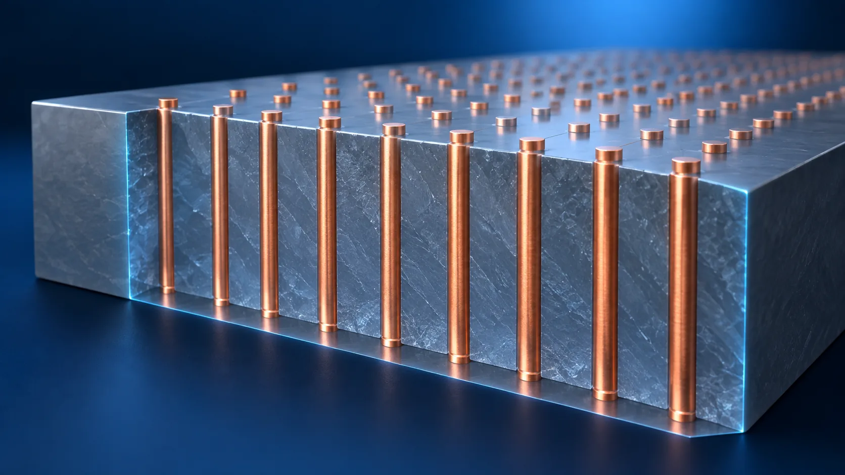
An electrode that runs straight through a chip. That is the whole description, and yet underneath it sit four layers of materials engineering: a dielectric liner, a barrier metal, plating chemistry and stress design.
- What a TSV is (the short version)
- Inside a TSV there is no single copper post
- How one gets built — seven steps
- When to build it: via-first, via-middle, via-last
- A materials engineer's view: copper misbehaves
- Change the dimensions and the material changes too
- Thinning, and revealing the via
- What is still hard
- Glossary / Primary sources / Claim-to-source audit
Sourced = a value stated in published material from a research institute or manufacturer (link given)
Our calculation = a figure this article derived, with the assumptions spelled out
Not yet confirmed = research-stage work with no confirmed production record
Beyond those, descriptions of how a process generally runs or why a physical mechanism works are marked Commentary.
1. What a TSV is (the short version)
A TSV (through-silicon via) is an electrode that passes right through a silicon chip, from the front face to the back, and connects what is above it to what is below.
- What it does: joins stacked chips by the shortest possible route
- Where it appears: the stacked DRAM in HBM, silicon interposers, 3D-stacked logic
- Why it is needed: wiring that has to travel around the edge of a chip is both too long and too few in number
The HBM article treats TSVs as the single component that makes HBM possible; the Die Stacking article treats them as the reason stacking requires thinning. This article is about the via itself: how you make one, and what materials problems come with it.
2. Inside a TSV there is no single copper post
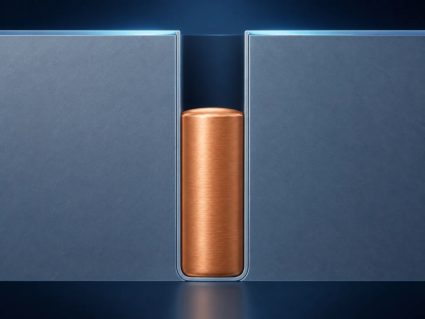
Drawn in a diagram, a TSV is almost always one copper rod. The real cross-section has far more layers than that.
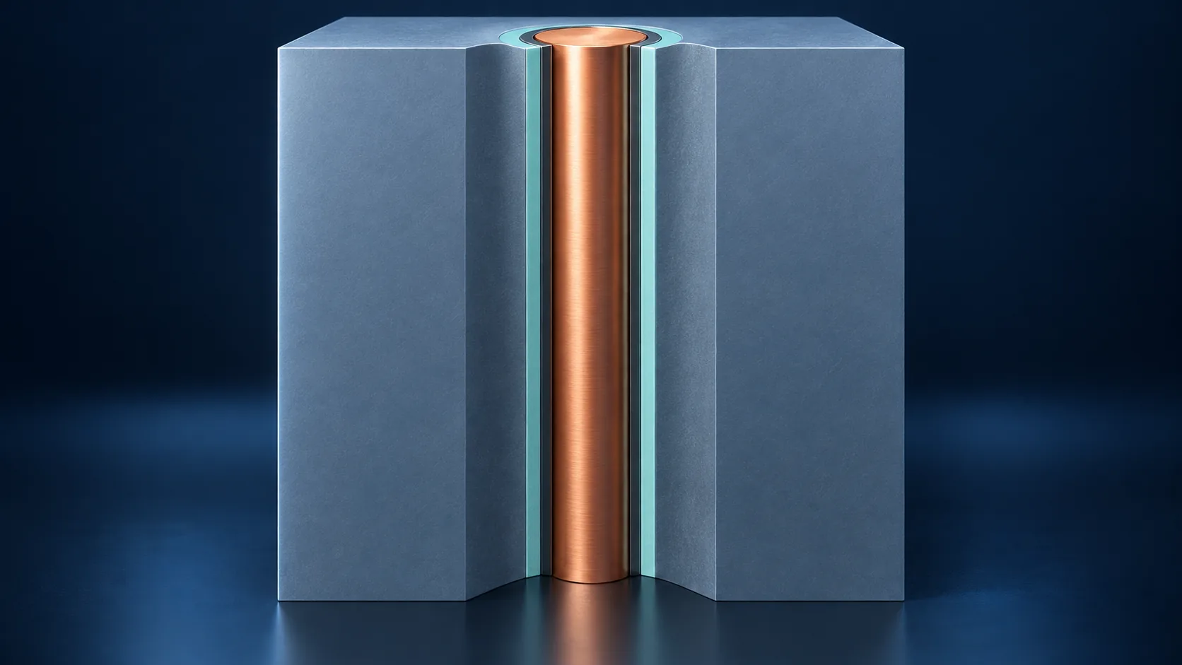
Copper diffuses through silicon. Once inside, copper atoms create deep levels that wreck transistor behaviour.
So any copper wiring needs a film that stops that diffusion. For a TSV, that film has to cover the entire sidewall of a hole tens of micrometres deep, with no gaps anywhere. Thin, uniform and unbroken, down the wall of a deep hole — that is where the deposition problem lives.
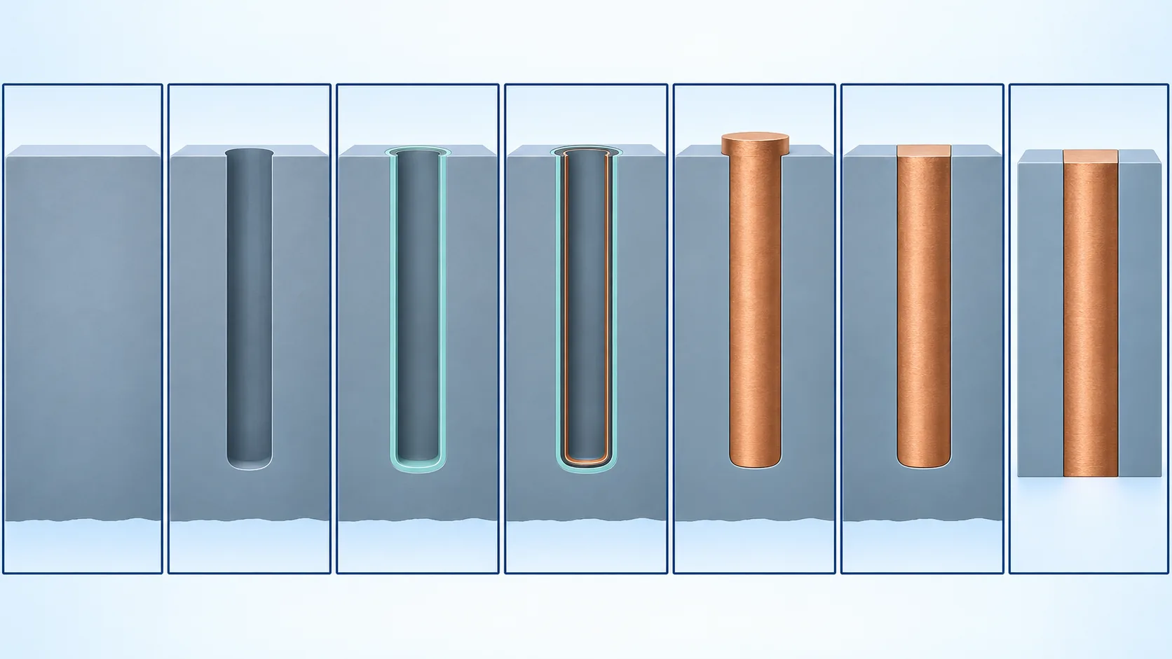
3. How one gets built — seven steps
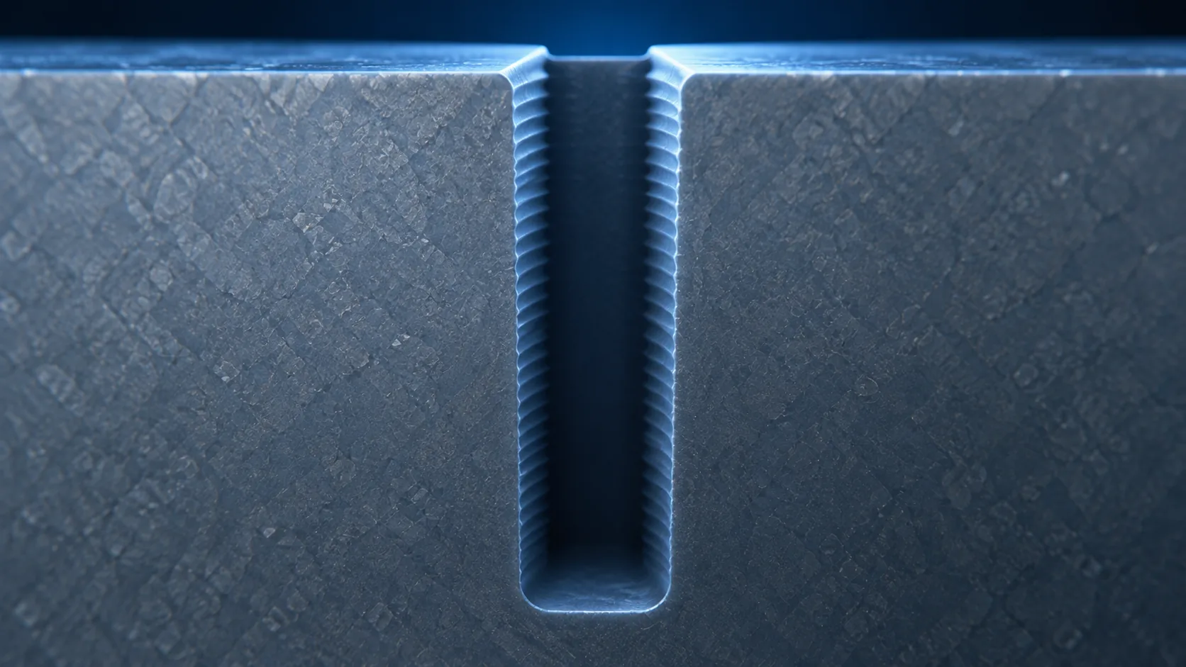
Step 1, the hole — the sidewall is not smooth
To cut a deep hole that stays vertical, the usual method is to alternate rapidly between an etching step and a step that protects the sidewall. The consequence is that the wall is left with a fine wavy texture, known as scalloping.
That texture matters later on. If the dielectric or the barrier film goes on thin in the troughs, those troughs become the weak points.
Step 4, the plating — it has to fill from the bottom
Electroplate metal into a narrow, deep hole and it normally grows faster near the entrance, because current reaches there more easily and metal ions are replenished more readily.
The result is that the mouth closes first and a void gets sealed inside. A void raises resistance and becomes the starting point for a crack under thermal cycling.
To prevent this, the plating bath carries several additives. They suppress deposition near the entrance and accelerate it at the bottom — varying the growth rate by position so the hole fills upward from the base. Plating looks like an electrical technology; in practice it is additive chemistry.
4. When to build it: via-first, via-middle, via-last
TSVs fall into three families depending on where in device manufacturing they are formed.
| Approach | When it is formed | Character |
|---|---|---|
| via-first | Before the transistors exist | Few constraints from later heat and chemistry, but the via must survive every subsequent step |
| via-middle | After the transistors, before the wiring | The approach widely used in production today |
| via-last | After the wiring is finished, usually from the back side | Least disturbance to a completed device, but it demands a low-temperature process |
The three-way classification is standard in the industry. The descriptions in the third column are this article's commentary.
imec's nano-TSV is via-last
In its demonstration of a backside power delivery network, imec formed nano-TSVs using a via-last approachSourced. The published process runs as follows (imec).
| Step | What imec states |
|---|---|
| Starting material | An epitaxial Si/SiGe stack is grown on a bulk Si substrate. The SiGe layer acts as an etch-stop that halts the later wafer thinning |
| Bonding | After device formation and wiring, the wafer is flipped and the active (front) face is joined to a second carrier wafer by low-temperature wafer-to-wafer bonding |
| Thinning | Final Si thickness of 20 to 370 nm |
| Fill material | n-TSV patterning and tungsten fill, followed by backside metallisation |
| Function | Connects backside metal-1 electrically to frontside metal-1 |
All Sourced (imec published article). This is research-stage work and does not indicate a production-level capability.
Note where the decision about "how far to grind" actually lives: not in the control of the tool doing the removing, but in the material being removed. The SiGe layer is placed there as a boundary at which the removal behaviour changes, so thickness control at the nanometre scale comes from a choice of material combination rather than from the precision of the grinder.
The TAIKO process seen in the Die Stacking article solves its problem with shape; this one solves it with composition. Both are answers that avoid "make the machine more precise".
5. A materials engineer's view: copper misbehaves
The best-known reliability problem with TSVs comes from the thermal expansion of copper.
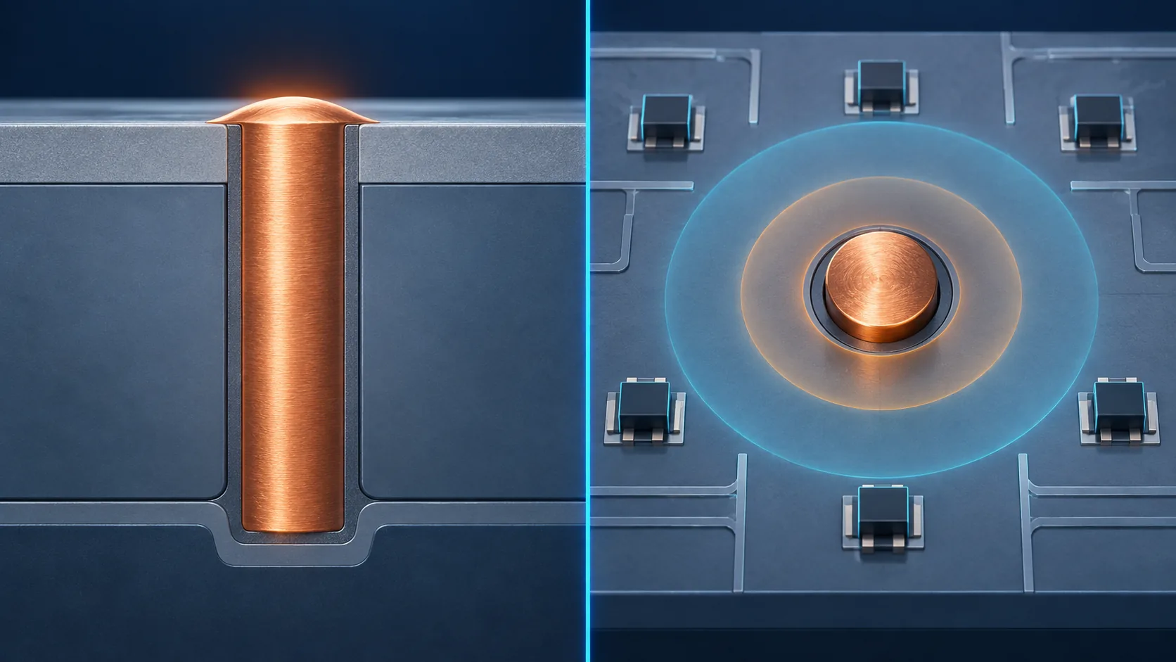
Copper expands more with temperature than silicon does. Copper trapped in a hole in silicon tries to grow when the temperature rises, and sideways there is nowhere to go. What is left is the vertical direction, so it is pushed out at the end face. That is what pumping means.
At the same time, the copper trying to expand presses on the silicon around it. Stress in silicon changes the carrier mobility of whatever transistors sit there, so a region around each TSV has to be left empty of devices.
A connection that is a point electrically occupies an area mechanically — which is why a TSV cannot be designed as if it were just another wire.
6. Change the dimensions and the material changes too
Return for a moment to the imec figures from Section 4. imec's nano-TSVs are filled with tungsten, not copperSourced.
Tungsten is a metal whose thermal expansion is smaller than copper's. As Section 5 showed, most TSV reliability problems trace back to copper expanding. If you intend to place nanometre-scale vias in large numbers right next to transistors, choosing a material that does not want to expand in the first place becomes the rational move.
The trade is that tungsten has higher electrical resistance than copper. In a wide, long via resistance dominates and copper wins; in a narrow, short via stress dominates and tungsten wins — that is how the split reads.
The name "TSV" stays the same, but when the dimensions move by orders of magnitude the best material moves with them. The term should not be treated as one thing; it is worth asking which size regime is being discussed.
7. Thinning, and revealing the via
Etching the hole does not by itself make the via go all the way through. The back of the wafer has to be removed until the buried metal shows its head.
Among the equipment that supports this step, Tokyo Electron offers the Synapse and Ulucus series for 3D integration, describing them as tools that enable temporary wafer bonding and debonding, plus permanent bonding, in the through-silicon via (TSV) manufacturing processSourced.
| Item | What Tokyo Electron states |
|---|---|
| Thickness handled | Stable transport and processing even for extremely thin wafers of 50 µm or less |
| Temporary bond and debond | Functions for coating, drying and bonding the material that temporarily joins two wafers, plus debonding and cleaning of both the device and carrier wafers |
| Placement accuracy | 3σ < 100 nm (Synapse™ Si) |
| Permanent bonding | Supports both fusion bonding and Cu hybrid bonding |
All Sourced (Tokyo Electron).
The same company lists the open problems in advanced packaging as managing wafer warpage, minimising post-bond distortion, and high-precision alignment and overlay metrologySourced (Tokyo Electron).
8. What is still hard
(1) Treating the inside of a deep hole uniformly
As Sections 2 and 3 showed, the liner, the barrier and the plating all have to be uniform inside a hole that is deep and narrow. The fact that conditions differ between the mouth and the bottom is the root difficulty of the whole technology.
(2) Reconciling stress with design
As Section 5 showed, a TSV imposes stress on its surroundings. The design side wants more vias for more bandwidth; the reliability side wants less stress. Those pull against each other.
(3) Handling thin wafers
Revealing a TSV requires thinning, and thinning makes the wafer fragile (covered in detail in the Die Stacking article). The reason Tokyo Electron offers temporary bonding and debonding tools for 3D integration is to avoid ever handling a thin wafer on its ownSourced.
(4) How this relates to hybrid bonding
Vertical connection once meant TSVs and nothing else. Direct face-to-face bonding is now in production as well, but the two are used together rather than in competition. Face bonding joins one die to another; getting through the inside of a die and out the other side still takes a TSV.
9. Glossary
- TSV
- Through-Silicon Via. An electrode that passes through silicon to connect the two faces.
- Liner (dielectric)
- The insulating layer applied to the hole wall, separating copper from silicon electrically.
- Barrier metal
- A metal film that stops copper diffusing into the silicon.
- Seed layer
- The thin metal layer that electroplating starts from.
- Bottom-up fill
- Depositing metal from the base of the hole upward so no void is left behind.
- Void
- A cavity left inside during filling. It raises resistance and seeds cracks.
- Scalloping
- The fine wavy texture left on the sidewall by deep reactive etching.
- Aspect ratio
- The ratio of hole depth to diameter. Higher means narrower and deeper.
- via-first / middle / last
- Classification by the stage of device manufacturing at which the TSV is formed.
- nano-TSV
- A TSV with nanometre dimensions, used for backside power delivery among other things.
- Etch-stop layer
- A layer inserted deliberately so removal behaviour changes there, fixing the end point of thinning.
- Pumping
- The bulging of a TSV end face caused by mismatched thermal expansion.
- Keep-out zone (KOZ)
- The region around a TSV where stress prevents devices from being placed.
- TSV reveal
- The step that removes the back face until the TSV heads appear.
- Temporary bond / debond
- Attaching a thin wafer to a carrier for the duration of a process, then releasing it.
10. Primary sources
- imec "Imec demonstrates critical building blocks for a backside power delivery network" — imec-int.com
- Tokyo Electron "3D Integration: Synapse™ / Ulucus™ series" (Japanese-language page) — tel.co.jp
- Tokyo Electron "The R&D front line TEL is opening up in the advanced packaging era", 30 September 2025 (Japanese-language page) — tel.co.jp
- TSMC "TSMC-SoIC®" technology page — 3dfabric.tsmc.com
- TSMC "CoWoS®" technology page — 3dfabric.tsmc.com
11. Claim-to-source audit
| Claim in the text | Basis | Label |
|---|---|---|
| imec's nano-TSV uses a via-last approach; the SiGe in an epitaxial Si/SiGe stack acts as the etch-stop for thinning; the wafer is flipped and joined to a carrier by low-temperature wafer-to-wafer bonding; final Si thickness is 20 to 370 nm; the n-TSV is filled with tungsten; it connects backside metal-1 to frontside metal-1 | imec published article[Source 1] https://www.imec-int.com/en/articles/imec-demonstrates-critical-building-blocks-backside-power-delivery-network | Sourced |
| Tokyo Electron Synapse / Ulucus: temporary bonding, debonding and permanent bonding for the TSV process; handles wafers of 50 µm or less; Synapse™ Si placement accuracy 3σ < 100 nm; supports both fusion and Cu hybrid bonding | Tokyo Electron product page[Source 2] https://www.tel.co.jp/product/synapse-ulucus.html | Sourced |
| The open problems in advanced packaging given as wafer warpage management, minimising post-bond distortion, and high-precision alignment and overlay metrology | Tokyo Electron blog, 30 September 2025[Source 3] https://www.tel.co.jp/blog/all/20250930_001.html | Sourced |
| The layer sequence of a TSV (silicon / dielectric liner / barrier metal / seed plus copper), the seven process steps, and the via-first, via-middle, via-last classification | Commentary: this article's summary of typical TSV structure and process. It does not describe any specific product | Commentary |
| That copper diffuses into silicon and degrades device behaviour, which is why a barrier metal is required | Commentary based on general semiconductor process knowledge | Commentary |
| That plating a deep hole closes the mouth first and leaves a void, and that additives vary the local deposition rate to achieve bottom-up fill | Commentary based on general electrochemical and plating mechanisms. No specific bath or condition is given | Commentary |
| That deep reactive etching leaves scalloping on the sidewall | Commentary based on general machining and etching knowledge | Commentary |
| That copper expands more than silicon, producing pumping and a keep-out zone, and that stress affects carrier mobility | Commentary based on general mechanisms in materials physics. No deformation magnitude, stress value or KOZ dimension is claimed | Commentary |
| That tungsten has lower thermal expansion and higher resistivity than copper, and that the best material can change with dimension | Commentary based on general properties of metals. imec did not state a reason for its material choice; this is our own reading | Commentary |
Last updated 20 September 2026. Sources are limited to primary material (official publications and product technology pages from research institutes and manufacturers). Because this article contains a good deal of general description of processes and physical mechanisms, those passages are marked Commentary to separate them from sourced fact. All figures are explanatory concept graphics. Visual-overview figures are shown as AI-generated conceptual images, matching the Japanese edition. Vector drawings are retained where they carry quantitative values or precision-critical technical labels. AI-generated images do not depict real equipment, products, facilities, dimensions or exact cross-sections; replaced source SVG overview drawings remain in the HTML but are hidden.