TECHNOLOGY EXPLAINER
What Interfacial Resistance Is
— the number that never appears in a material datasheet
The hardest opponent in an all-solid-state battery is not the material but the boundary between materials. What makes it awkward is that the resistance is not settled once you have chosen the materials. For one and the same pair, a factor of 33 has been reported.

- What interfacial resistance is (the short version)
- Why resistance arises at an interface — three causes
- A materials engineer's view (1): what the unit Ω cm² is telling you
- A factor of 33 for the same materials — interfacial resistance is set by process
- The culprit was not a gap but a chemical reaction layer
- Our calculation: what interfacial resistance takes from a cell
- Four ways to rebuild the interface
- A materials engineer's view (2): what cannot be measured cannot be made
- What is still hard
- Glossary / Primary sources / Claim-to-source audit
Sourced = a value stated in published material from a research institute or manufacturer (link given)
Our calculation = a figure this article derived, with the assumptions spelled out
Not yet confirmed = a plan or a target with no confirmed production record
Structural readings and materials-design interpretations are marked separately as Commentary.
1. What interfacial resistance is (the short version)
Interfacial resistance is the difficulty ions have in crossing the boundary between two materials. In an all-solid-state battery, that boundary resistance ends up deciding the performance of the whole cell.
- Where it arises: between the cathode active material particles and the solid electrolyte, and between the solid electrolyte and the anode. There are countless such boundaries inside a cell
- Why it matters: a JST joint announcement states that the low lithium-ion conductivity at the interface formed between solid electrolyte and electrode (high interfacial resistance) is a major problem for practical use, and that if resistance at the interface is high, a good battery capable of fast charge and discharge cannot be developedSourced
- What makes it awkward: choosing the material does not fix the value. For the same pair of materials, 5.5 Ω cm² and 180 Ω cm² have both been reportedSourced. The difference was not the material but how the surface was made
Where interface resistance arises
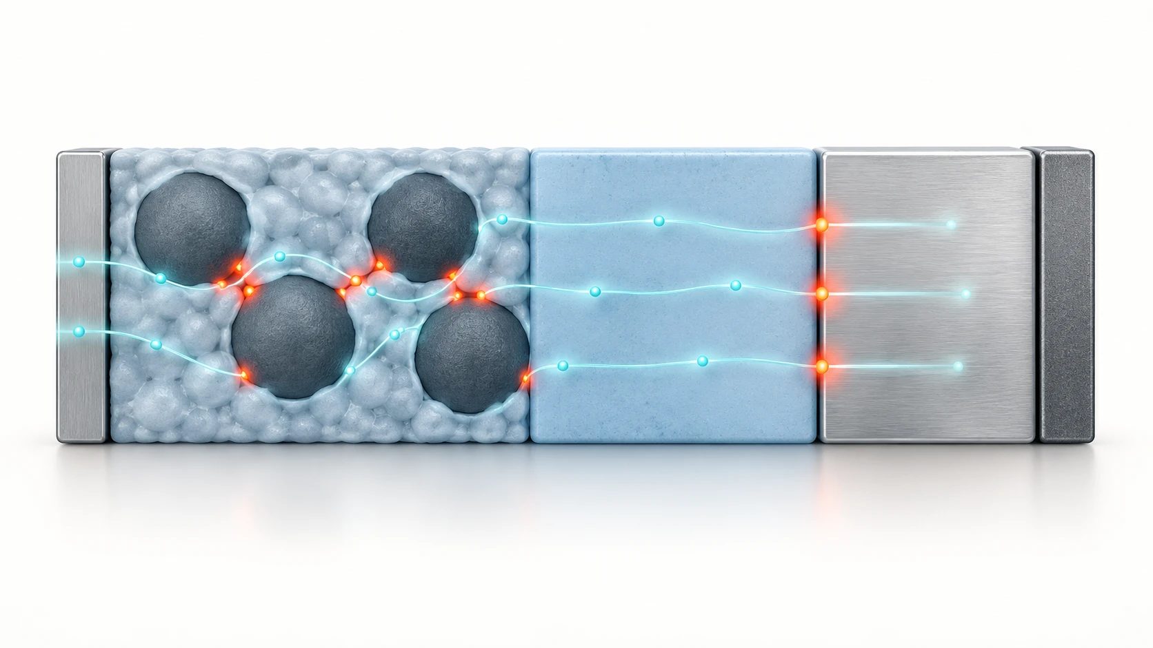
- Composite cathode: many contacts between active particles and solid electrolyte
- Anode side: a planar boundary between solid electrolyte and lithium metal
Interfacial resistance is not a material property. It is a quantity set by how you make it. Which is why it does not appear in a material catalogue. And precisely because it does not, this is where companies differ.
2. Why resistance arises at an interface — three causes
"Resistance rises at the boundary" is one sentence, but the cause is not single. Set the published results side by side and at least three separate reasons appear.
Three causes of interfacial resistance
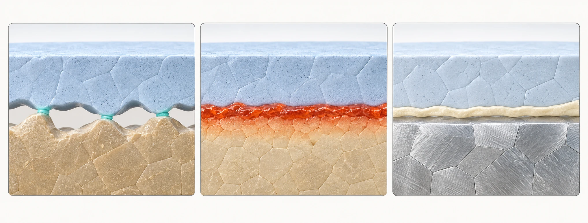
- Insufficient contact: solids touch at limited points, leaving too little true contact area
- Reaction layer: structural change and sulfur diffusion extend about 10 nm from the LiCoO2 surface
- Insulating film: a Li2CO3 layer on LLZO produces high interfacial resistance
| Cause | As the published material puts it | Source |
|---|---|---|
| 2 Chemical reaction layer | When a sulfide solid electrolyte meets an electrode material, structural change and sulfur diffusion occur to a depth of about 10 nm from the LiCoO2 electrode surface. That is the chemical reaction layer, and when it is present at the interface it produces extremely high interfacial resistance | Tokyo Institute of Technology and the University of Tokyo (July 2022) |
| 3 Insulating surface film | An insulating lithium carbonate layer (Li2CO3) forming on the surface produces high interfacial resistance, and this has been a major obstacle to practical use | Tohoku University (March 2026) |
| (For reference) interface fracture | Repeated charging and discharging produces cracks between the cathode or anode and the solid electrolyte, degrading cell performance | Toyota (October 2023) |
All Sourced (Tokyo Institute of Technology [Source 3], Tohoku University [Source 5], Toyota [Source 8]).
1 is a mechanical problem: press harder, use a softer material, control the particle size distribution — solve it with mechanics.
2 is a chemical problem: choose a partner that does not react, or put a layer between them that stops the reaction.
3 is a process-control problem: keep it out of the air, or remove what the air left behind.
Summarising all of it as "interfacial resistance is high" hides that difference in remedy. In real development, working out which cause dominates is where the contest is (our commentary).
3. A materials engineer's view (1): what the unit Ω cm² is telling you
Almost without exception, published interfacial resistances are given in Ω cm². Not Ω, and not Ω cm. The character of the quantity is right there in the unit.
Bulk resistance, inside a material, is proportional to thickness. So it is written as a resistivity in Ω cm, and dividing by the thickness gives the actual resistance. Make it thinner and it falls.
An interface has no thickness. It has only area. So it is written as a resistance per unit area, Ω cm². Divide by the area and you get the actual resistance. Making things thinner does not reduce it.
Take the high-resistance value of 180 Ω cm² reported by Tokyo Institute of TechnologySourced and apply it to an electrode of a given sizeOur calculation.
- Assumption: take the electrode area as 10 cm × 10 cm = 100 cm²
- 180 Ω cm² divided by 100 cm² = 1.8 Ω
- For the same electrode, the low-resistance 5.5 Ω cm² gives 5.5 divided by 100 = 0.055 Ω
Assumptions and limits: that division assumes a single interface spread uniformly over the full electrode area. In a real electrode, every active material particle has its own interface. The total particle surface area is far larger than the apparent electrode area, while only part of it is actually in contact. This calculation exists only to show what the unit means; it is not an estimate of the internal resistance of a real cell.
Because Ω cm² is per unit area, there are in principle only two ways to lower the actual resistance.
- (A) Increase the area — finer particles, closer adhesion, more pressure
- (B) Lower the Ω cm² value itself — rebuild the chemistry and structure of the interface
What is easy to miss is that raising the ionic conductivity of the solid electrolyte is neither of them. Conductivity is S/cm; interfacial resistance is Ω cm². Different dimensions, so improving one does not move the other.
The situation where materials people race for champion conductivity data while cell performance does not improve comes from exactly that difference in dimension. Conductivity and interfacial resistance are contests in different arenas (our commentary).
4. A factor of 33 for the same materials — interfacial resistance is set by process
In November 2018 a group from Tokyo Institute of Technology, Nippon Institute of Technology and AIST published a result that changed how this field is seenSourced.
With the cathode material lithium cobalt oxide (LiCoO2) and the solid electrolyte lithium phosphate (Li3PO4) — the same pair of materials — the interfacial resistance came out at 5.5 Ω cm² in one case and 180 Ω cm² in anotherSourced.
| State of the interface | Interfacial resistance | Material pair |
|---|---|---|
| Low-resistance interface | 5.5 Ω cm² (described as an extremely low value) | LiCoO2 / Li3PO4 |
| High-resistance interface | 180 Ω cm² | LiCoO2 / Li3PO4 (the same) |
| Difference | about 33 timesOur calculation | Identical materials. What differed was the state of the surface |
The 5.5 and 180 Ω cm² are Sourced (Tokyo Institute of Technology [Source 1], JST joint announcement [Source 2]). "About 33 times" is this article rounding 180 divided by 5.5 = 32.7.
What was different? According to the announcement, the key was a regular atomic arrangement at the electrode surfaceSourced. The group grew an epitaxial LiCoO2 thin film on an Al2O3 single-crystal substrate, making the interface with the surface atoms alignedSourced.

Material properties — density, melting point, elastic modulus, ionic conductivity — are fixed once the material is. So they can go in a catalogue.
Interfacial resistance cannot. The same material name moves by a factor of 33. At best it could be listed with the caveat "when made under our recommended conditions".
For a materials business that carries real weight. Selling the material alone does not deliver the material's performance. Surface treatment conditions, mixing, compaction — unless the method goes with it, the value does not reproduce at the customer.
That is why solid electrolyte makers work so closely with cell makers, and why cathode material makers take on surface coating themselves (our commentary).
5. The culprit was not a gap but a chemical reaction layer
In July 2022, Specially Appointed Associate Professor Kazunori Nishio and graduate student Daisuke Imazeki of the School of Materials and Chemical Technology at Tokyo Institute of Technology, with Professor Taro Hitosugi of the Graduate School of Science at the University of Tokyo, announced that they had identified the origin of interfacial resistanceSourced.
When a sulfide solid electrolyte meets an electrode material and forms an interface, structural change and sulfur diffusion occur to a depth of about 10 nm from the LiCoO2 electrode surface. That is the chemical reaction layer, and when it is present at the interface it produces extremely high interfacial resistance. (Tokyo Institute of Technology news, July 2022)
And the remedy was startlingly simple. Introducing a Li3PO4 solid electrolyte about 10 nm thick as a buffer layer between Li3PS4 and LiCoO2 cut the internal resistance of the cell to 1/2,800 of its previous valueSourced.
To feel what 10 nm is, compare it with the thickness of an electrodeOur calculation.
- Assumption: take the electrode layer as 100 µm thick (typical of lithium-ion electrodes)
- 100 µm = 100,000 nm
- 10 nm divided by 100,000 nm = 1/10,000
A layer one ten-thousandth of the thickness was deciding the resistance of the whole cell.
Assumptions and limits: the 100 µm electrode is our own assumption; designs range from tens to hundreds of micrometres. And the 1/2,800 reduction is a value obtained in a thin-film test cell; it does not show that the same ratio holds in a production cell.
From the materials side, this becomes the requirement to put a 10 nm film evenly on every individual particle. Depositing 10 nm on a flat substrate and depositing 10 nm over the entire surface of a powder are quite different difficulties (our commentary).
6. Our calculation: what interfacial resistance takes from a cell
A number in Ω cm² does not by itself say whether it is large or small. Convert it into voltage. The drop when a current density j (A/cm²) passes an area resistance R (Ω cm²) is ΔV = j × R.
- Take the areal capacity of the electrode as 3 mAh/cm² (typical of lithium-ion electrodes)
- Then 1C = 3 mA/cm² = 0.003 A/cm² and 3C = 9 mA/cm² = 0.009 A/cm²
- Take the working voltage of the cell as 3.7 V
- Use ΔV = j × R for the drop at one interface
| Interfacial resistance (published) | ΔV at 1C (3 mA/cm²) | ΔV at 3C (9 mA/cm²) | Share of 3.7 V (at 1C) |
|---|---|---|---|
| 1.5 Ω cm² (Li/LLZO with Au layer) | 0.005 V | 0.014 V | about 0.1% |
| 5.5 Ω cm² (LiCoO2/Li3PO4, low) | 0.017 V | 0.050 V | about 0.4% |
| 10.3 Ω cm² (air exposure then heating) | 0.031 V | 0.093 V | about 0.8% |
| 180 Ω cm² (LiCoO2/Li3PO4, high) | 0.54 V | 1.62 V | about 15% |
| 225 Ω cm² (Li/LLZO, ultrasonic only) | 0.68 V | 2.03 V | about 18% |
The interfacial resistances are Sourced (published by the respective institutions). The ΔV values and shares are Our calculation.
A single interface at 180 Ω cm² loses 0.54 V at 1C, an entirely ordinary rate of charge and discharge. That is about 15% of a 3.7 V cellOur calculation.
And the lost voltage becomes heat. At 3C (9 mA/cm²) it is 1.62 V — no longer a working battery at all. JST's statement that a good battery capable of fast charge and discharge cannot be developed if interfacial resistance is high means exactly this, put into numbersSourced.
Assumptions and limits: this estimate looks at one interface only. A real cell has interfaces on the cathode and anode sides, and inside the cathode composite every active material particle has one. The real loss is larger. And changing the assumptions for areal capacity, cell voltage or C-rate changes the values.
7. Four ways to rebuild the interface
Sorting the published countermeasures, there are broadly four directions.
| Approach | Interface addressed | Published result | Source |
|---|---|---|---|
| Introducing a buffer layer | Li3PS4 / LiCoO2 | Inserting Li3PO4 about 10 nm thick cut the internal resistance of the cell to 1/2,800 of its previous value | Tokyo Institute of Technology and the University of Tokyo (July 2022) |
| Heat treatment | Li3PO4 / LiCoO2 | An interface degraded by air exposure was recovered by heating at about 150 °C, giving 10.3 Ω cm² (comparable with 10.9 Ω cm² without exposure), less than a tenth of the value before heating | Tokyo Institute of Technology and others (January 2022) |
| Ultrasonic bonding | Li metal / LLZO | Bonded at room temperature in seconds. Interfacial resistance about 225 Ω cm², and about 1.5 Ω cm² with a thin Au layer as well | Tohoku University (March 2026) |
| Uniform surface coating | The surface of cathode active material particles | For LiNbO3 coating on NMC622 particles, an evaluation technology was established that visualises coating thickness as a map over a target range of 6 to 20 nm | JFE Techno-Research (September 2025) |
All Sourced (Tokyo Institute of Technology [Sources 3 and 4], Tohoku University [Sources 5 and 6], JFE Techno-Research [Source 7]).
What deserves attention in the Tohoku University result (3) is what the cause of the interfacial resistance turned out to be. The announcement says that in bonding lithium metal to LLZO, an insulating lithium carbonate layer (Li2CO3) forming on the surface produces high interfacial resistance, and this has been a major obstacle to practical useSourced.
Oxide solid electrolytes are usually described as chemically stable and easy to handle in air. In fact, they had been reacting with components of the air and building an insulating layer on the surface.
A material being resistant to air and an interface being sound are two different statements. Even if the bulk does not decompose, a few nanometres of altered surface send the interfacial resistance up (our commentary).
Point 4 is more surprising still. An interface degraded by exposure to air was reported to be improved by heating at about 150 °C to performance equivalent to a cell never exposed to airSourced. Interface degradation is not necessarily irreversible damage. That bears directly on production line design: "never let it touch air" is not the only answer; "restore it after it has" is a possible option (our commentary).
8. A materials engineer's view (2): what cannot be measured cannot be made
Everything so far converges on how to make a layer of around 10 nm. So how do you confirm that the layer really is where you intended?
In September 2025, JFE Techno-Research announced that it had established an evaluation technology for the coverage uniformity of coating layers on electrode active material surfacesSourced. NMC622 cathode active material particles were coated with a niobium-based coating material (LiNbO3), with target thicknesses varied across 6 to 7 nm, 7 to 10 nm, 14 to 16 nm and 17 to 20 nm, and the method visualises the coating thickness as a mapSourced.
The method displays an image acquiring, at the same time, elemental information from high-sensitivity energy-dispersive X-ray spectroscopy (EDX) and structural information from the backscattered electron image of a scanning electron microscope (SEM), and visualises the thickness of the coating film as a map by superimposing, on the SEM image, information converted into thickness from the characteristic X-rays emitted by specific elements in the coating material. As background it notes that securing sufficient contact points between solid particles to ensure ionic and electronic conduction is important, but that quantitatively evaluating the character of this extremely thin coating layer is difficult (JFE Techno-Research, 10 September 2025)Sourced.
"We have established a technology for measuring film thickness" being a news release means that until then it could not be measured.
As Section 5 showed, what sets interfacial resistance is a layer of around 10 nm. The means of quantifying how that layer's thickness varies from particle to particle only began to come together in 2025.
In materials development, evaluation technology often sets the ceiling on development speed. If you cannot see the variation, varying the conditions tells you nothing about what worked. Since interfacial resistance is set by process, without a yardstick for how well the process went, improvement is guesswork (our commentary).
The point in Section 4 about not being able to put it in a catalogue also means, in reverse, that the party holding the evaluation technology is the strong one.
9. What is still hard
(1) Almost no values from production cells are published
Every interfacial resistance figure this article could confirm comes from a thin-film test cell or an experiment using a particular bonding methodSourced. Values for interfacial resistance in an actual production cell could not be found in published primary sources within the scope of this article and are not stated. The five values in Fig. 3 also differ in material system, sample geometry and measurement conditions.
(2) The distance between an interface made on a plane and one made on powder
The Tokyo Institute of Technology results use epitaxial thin films grown on an Al2O3 single-crystal substrateSourced. That is a design for seeing what happens at an ideal interface with the atoms aligned. Production electrodes, by contrast, are aggregates of powder with the particles in random orientations. Whether guidance confirmed in thin films carries over unchanged to powder could not be confirmed within the scope of this article (our commentary).
(3) The interface after repeated cycling
Toyota states that repeated charging and discharging produces cracks between the cathode or anode and the solid electrolyte, degrading cell performanceSourced. Every interfacial resistance value in this article belongs to an interface as made. How interfacial resistance changes after continued use could not be confirmed numerically in published primary sources.
- Interfacial resistance is not a material property. For the same LiCoO2/Li3PO4 pair, 5.5 and 180 Ω cm² have both been reportedSourced
- The unit Ω cm² (area resistance) is the essential point. Raising bulk ionic conductivity (S/cm) does not lower interfacial resistance (our commentary)
- The culprit was not only a gap. In sulfide systems a chemical reaction layer of about 10 nm had formed at the interfaceSourced
- A 10 nm buffer layer took the internal resistance of the cell to 1/2,800. A layer about one ten-thousandth of the electrode thickness was deciding the wholeOur calculation
- 180 Ω cm² takes about 0.54 V at 1C, about 15% of a 3.7 V cellOur calculation
- Oxides are called air-stable, yet a lithium carbonate layer forms on the surface. Material stability and interface soundness are different thingsSourced
10. Glossary
- Interfacial resistance
- Electrical resistance arising at the boundary between materials. One of the main things governing all-solid-state battery performance.
- Area-specific resistance (Ω cm²)
- Resistance per unit area, the unit for parts with no thickness, such as an interface.
- Ionic conductivity (S/cm)
- How readily ions move through a material. A quantity of different dimension from interfacial resistance.
- Chemical reaction layer
- The altered layer formed at an interface when different materials meet. Here it means sulfur diffusion and structural change.
- Buffer layer
- A thin layer inserted at an interface to prevent reaction. Here, Li3PO4 about 10 nm thick.
- Epitaxial thin film
- A film grown with its crystal orientation aligned to the substrate, allowing an interface with controlled atomic arrangement.
- LLZO
- The garnet-type oxide solid electrolyte Li7La3Zr2O12, regarded as chemically stable.
- Lithium carbonate (Li2CO3)
- An insulating surface layer formed by reaction with components of the air. A source of interfacial resistance.
- Ultrasonic bonding
- Joining materials with ultrasonic vibration, without heating or melting.
- LiNbO3 coating
- A niobium-based coating applied to cathode active material particles, used at thicknesses of a few to 20 nm.
- Areal capacity (mAh/cm²)
- Capacity per unit area of electrode. The basis for converting current density into a C-rate.
- C-rate
- 1C is the current that uses the capacity in one hour. 3C empties it in about 20 minutes.
11. Primary sources
- Tokyo Institute of Technology "The bottleneck to all-solid-state batteries explained: guidance for lowering interfacial resistance established, opening the way to practical use", November 2018 (Japanese-language page) — titech.ac.jp
- Japan Science and Technology Agency (JST) Joint announcement "The bottleneck to all-solid-state batteries explained: guidance for lowering interfacial resistance established, opening the way to practical use", 23 November 2018 (Japanese-language release) — jst.go.jp
- Tokyo Institute of Technology "Origin of interfacial resistance in all-solid-state lithium batteries identified: interfacial resistance cut to 1/2,800, contributing to further performance gains", July 2022 (Japanese-language page) — titech.ac.jp
- Tokyo Institute of Technology "All-solid-state battery performance greatly improved by heat treatment, with hopes for application to electric vehicle batteries", January 2022 (Japanese-language page) — titech.ac.jp
- Tohoku University "Interface between lithium metal and a garnet-type oxide solid electrolyte formed at room temperature in a short time: a new method to push all-solid-state batteries towards practical use", 24 March 2026 (Japanese-language release) — tohoku.ac.jp
- Tohoku University Graduate School of Engineering "Interface between lithium metal and a garnet-type oxide solid electrolyte formed at room temperature in a short time" (Japanese-language page) — eng.tohoku.ac.jp
- JFE Techno-Research "Evaluation technology established for the coverage uniformity of coating layers on electrode active material surfaces, which govern all-solid-state battery performance", 10 September 2025 (Japanese-language release) — jfe-tec.co.jp
- Toyota Motor "Idemitsu and Toyota begin collaboration towards volume production of all-solid-state batteries for battery EVs", 12 October 2023 (Japanese-language release) — global.toyota
12. Claim-to-source audit
| Claim in the text | Basis | Label |
|---|---|---|
| That at the LiCoO2 and Li3PO4 interface the low-resistance case was an extremely low 5.5 Ω cm² and the high-resistance case 180 Ω cm²; that the key was a regular atomic arrangement at the electrode surface; that an epitaxial LiCoO2 thin film on an Al2O3 single-crystal substrate was used; and that the work appeared in ACS Applied Materials and Interfaces on 22 November 2018 (US time) | Tokyo Institute of Technology news, November 2018[Source 1] https://www.titech.ac.jp/news/2018/042963 | Sourced |
| That the low lithium-ion conductivity at the interface between solid electrolyte and electrode (high interfacial resistance) is a major problem for practical use; that a good battery capable of fast charge and discharge cannot be developed if interfacial resistance is high; and the composition of the research group (Professor Taro Hitosugi of Tokyo Institute of Technology, Professor Susumu Shiraki of Nippon Institute of Technology, Senior Researcher Tetsuroh Shirasawa of AIST) | JST joint announcement, 23 November 2018[Source 2] https://www.jst.go.jp/pr/announce/20181123/index.html | Sourced |
| That when a sulfide solid electrolyte meets an electrode material, structural change and sulfur diffusion occur to about 10 nm depth from the LiCoO2 surface, that this is the chemical reaction layer, and that its presence produces extremely high interfacial resistance; that introducing a Li3PO4 solid electrolyte about 10 nm thick as a buffer layer at the Li3PS4 and LiCoO2 interface cut the internal resistance of the cell to 1/2,800; and the researchers and journal | Tokyo Institute of Technology news, July 2022[Source 3] https://www.titech.ac.jp/news/2022/064488 | Sourced |
| That a cell exposed to air was improved by heat treatment at about 150 °C to performance equivalent to a cell not exposed to air; that the interfacial resistance after heating was 10.3 Ω cm², less than a tenth of the value before heating; and that the value without air exposure was 10.9 Ω cm² | Tokyo Institute of Technology news, January 2022[Source 4] https://www.titech.ac.jp/news/2022/062764 | Sourced |
| That in bonding lithium metal to LLZO an insulating lithium carbonate layer (Li2CO3) on the surface produces high interfacial resistance and has been a major obstacle to practical use; that ultrasonic bonding formed the interface at room temperature in seconds, giving about 225 Ω cm², and about 1.5 Ω cm² with a thin Au layer; and the announcement date of 24 March 2026 with publication in Small Structures | Tohoku University press release, 24 March 2026[Source 5] https://www.tohoku.ac.jp/japanese/2026/03/press20260324-02-Lithium.html | Sourced |
| That the same values (about 225 Ω cm², and about 1.5 Ω cm² with an Au layer) were confirmed on the Tohoku University Graduate School of Engineering page | Tohoku University Graduate School of Engineering news[Source 6] https://www.eng.tohoku.ac.jp/news/detail-,-id,3532.html | Sourced |
| That for LiNbO3 coating of NMC622 cathode active material particles an evaluation technology was established over target thicknesses of 6 to 7 nm, 7 to 10 nm, 14 to 16 nm and 17 to 20 nm, visualising coating thickness as a map; that the method acquires EDX and SEM backscattered electron images simultaneously; and the statements that securing sufficient contact points between solid particles to ensure ionic and electronic conduction is important, and that quantitatively evaluating the character of this extremely thin coating layer is difficult | JFE Techno-Research news release, 10 September 2025[Source 7] https://www.jfe-tec.co.jp/information/release/r20250910.html | Sourced |
| That repeated charging and discharging produces cracks between the cathode or anode and the solid electrolyte, degrading cell performance, and that the release is dated 12 October 2023 | Toyota newsroom[Source 8] https://global.toyota/jp/newsroom/corporate/39898897.html | Sourced |
| Putting the ratio of 180 to 5.5 Ω cm² at about 33 times (180 divided by 5.5 = 32.7); converting 180 Ω cm² on a 100 cm² electrode to 1.8 Ω; putting 10 nm at 1/10,000 of a 100 µm electrode thickness; and converting each interfacial resistance into a voltage drop with ΔV = j × R (1.5 to 0.005 V, 5.5 to 0.017 V, 10.3 to 0.031 V, 180 to 0.54 V, 225 to 0.68 V, with three times those values at 3C) and the shares of 3.7 V (about 0.1%, 0.4%, 0.8%, 15% and 18%) | Our calculation. The 100 cm² area, the 100 µm electrode thickness, the areal capacity of 3 mAh/cm² and the cell voltage of 3.7 V are all assumptions set by this article and are not published values. These are also values for one interface, and since a real cell has many, the actual loss is larger | Our calculation |
| Specific values of interfacial resistance in production cells | No published primary source stating interfacial resistance for a production cell could be confirmed within the scope of this article, so no such number appears in the text. Every value given is from a thin-film test cell or an experiment with a particular bonding method | Commentary |
| How much interfacial resistance changes after repeated cycling | The formation of cracks is published, but no numerical value for interfacial resistance after cycling could be confirmed within the scope of this article, so none is given | Commentary |
| Grouping the causes of interfacial resistance into insufficient contact, a chemical reaction layer and an insulating surface film; reading from the unit Ω cm² that improving bulk conductivity does not lower interfacial resistance; the point that interfacial resistance cannot go in a material catalogue; the point that whether thin-film guidance carries over to powder cannot be confirmed; the reading that evaluation technology sets the ceiling on development speed; and grouping the countermeasures into four | Our summary and commentary based on published content. Not views expressed by the institutions | Commentary |
| That Figs. 1, 2, 3, 5, 6 and 7 are explanatory concepts rather than real observations or design drawings, and that Figs. 1, 2 and 4 and the hero image are AI-generated | Our note | Commentary |
Last updated 21 September 2026. Sources are limited to primary material (official announcements from universities, public research institutes and companies). Because the article includes structural readings and materials-design interpretations, those are marked as Commentary and kept separate from sourced fact. Interfacial resistance values for production cells, and values after repeated cycling, are not stated here because no published primary source could be confirmed. The values set side by side in Fig. 3 differ in material system, sample geometry and measurement conditions and are not a ranking. All figures are explanatory concept graphics. Figs. 3, 5, 6 and 7 are vector drawings; Figs. 1, 2 and 4 and the hero image are AI-generated images, and none of them shows a real cross-section, micrograph or physical product.