

Key Findings
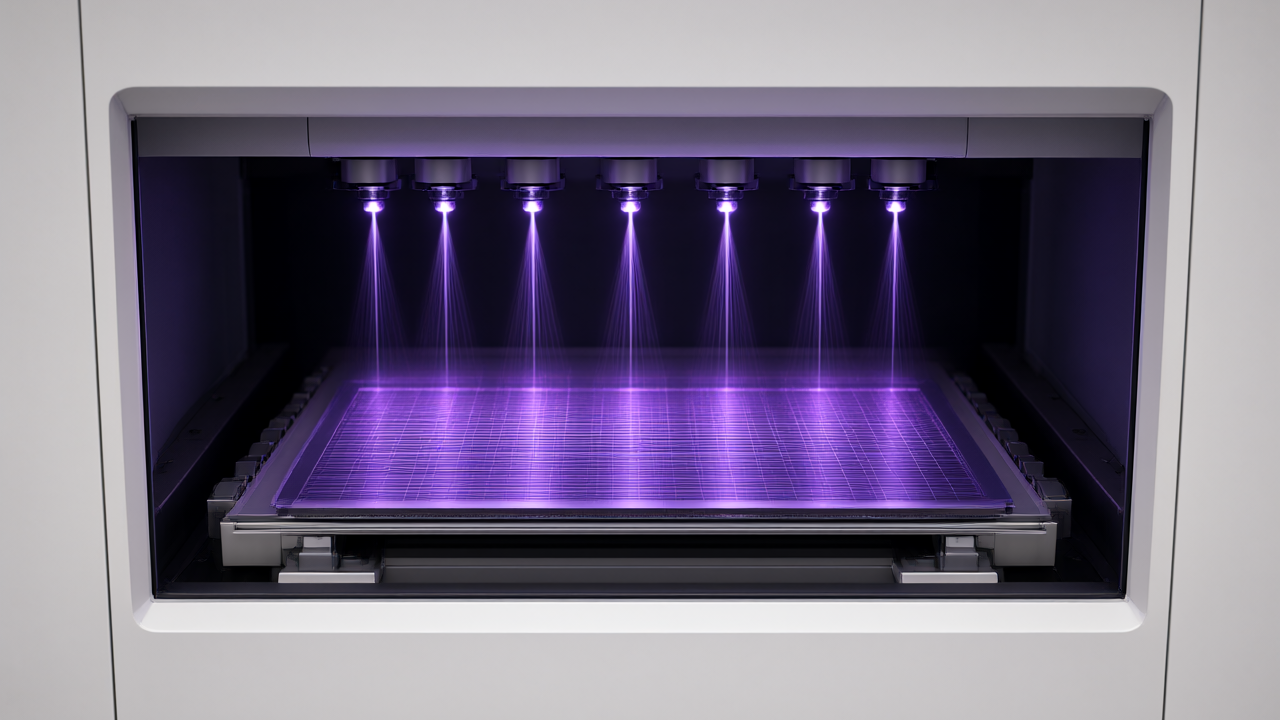
Nikon announced the upcoming launch of the DSP-110, a digital exposure system designed for semiconductor advanced packaging. Scheduled for release in April 2027, the device provides a resolution of 1.5μm (L/S). A primary technical advantage is its flexibility; the system can be modified to achieve a 1.0μm resolution by replacing the optical system to meet future process requirements.
Technical Details
The DSP-110 utilizes an i-line equivalent light source and achieves a throughput of 72 panels per hour for 510×515mm substrates. By redesigning the optical system for 1.5μm resolution, Nikon has improved throughput by approximately 40% compared to the DSP-100. The system maintains an overlay accuracy of ±0.3μm or less.
The device supports a wide range of substrate sizes, including:
- Square substrates: 310×310mm, 510×515mm, 600×600mm, and 730×920mm
- Wafers: 300mm
Additionally, the redesigned optical system expands the focus margin, which is intended to stabilize patterning across diverse substrate conditions and improve yield.
Background and Context
The development of the DSP-110 responds to the growing demand for high-density wiring in multi-layer FC-BGA substrates and large interposers within the advanced packaging market. This has increased the importance of Redistribution Layer (RDL) exposure technology. Nikon’s strategy involves providing digital exposure solutions that eliminate the need for photomasks while balancing high resolution with productivity. The DSP-110 follows the previously released DSP-100, which offers 1.0μm resolution and supports 600mm square substrates.
Significance and Outlook
The DSP-110 is positioned to reduce total costs and increase production efficiency for manufacturers. Because the system allows for a resolution upgrade to 1.0μm, it provides a roadmap for users to adapt to the increasing resolution requirements expected as advanced packaging technology evolves.
Source: https://monoist.itmedia.co.jp/mn/articles/2610/19/news040.html
Get our weekly technology intelligence — free
Receive an infographic that lets you judge at a glance whether each field’s analysis report is worth reading.
Subscribe Free — Weekly Tech Intelligence
By subscribing, you’ll receive Troy-Technical’s weekly technology intelligence newsletter.
- Your email and selected fields are used only to deliver the newsletter.
- We never share your information with third parties.
- You can unsubscribe anytime via the link in each email.
See our Privacy Policy for details.
Takes about a minute · Unsubscribe anytime