
Key Findings
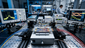
Researchers at Zhejiang University have reported a silicon photonic interconnect architecture capable of an aggregate bandwidth of 3.2 terabits per second. Published in PhotoniX Synergy, the work details a complete transceiver circuit designed for the O-band wavelength window. The system utilizes a combination of hybrid wavelength-port multiplexing, low-crosstalk multiplexing/demultiplexing, and adaptive wavelength stabilization to enable terabit-scale optical I/O for next-generation AI computing.
Technical Details
The architecture employs a heterogeneous design to balance bandwidth and physical footprint:
- Transmitter: Uses broadband lattice-filter-based multiplexers consisting of cascaded interferometric stages to ensure wide operating tolerance and controlled passbands.
- Receiver: Utilizes compact Vernier dual-microring demultiplexers, which use mismatched free spectral ranges of paired ring resonators to reduce chip area compared to conventional filter banks.
- Hybrid Multiplexing: The system scales capacity across two axes: wavelength multiplexing (stacking channels on different colors of light) and port multiplexing (duplicating this across multiple physical waveguide ports).
This dual-axis approach allows aggregate bandwidth to scale as the product of the number of wavelengths per port and the number of ports, preventing excessive channel density on a single waveguide.
Background and Context
Modern AI workloads generate massive data traffic between processors, memory banks, and servers. Traditional electrical interconnects using copper links face severe energy and bandwidth constraints as AI models grow and scale across thousands of accelerators. Silicon photonics mitigates these bottlenecks by encoding data onto light and guiding it through silicon waveguides, which offer lower loss and higher bandwidth density over distance.
Significance and Outlook
According to corresponding author Professor Jianyi Yang, the goal was to create a robust and scalable terabit-scale interconnect. By integrating complementary multiplexer designs and hybrid multiplexing, the team aims to increase capacity without requiring exotic packaging or extreme thermal control. This architecture provides a pathway to scale hardware proportionately with capacity increments, addressing the critical data-movement bottleneck in large-scale AI infrastructure.
Source: https://bioengineer.org/silicon-photonics-chip-hits-3-2-terabits-per-second-for-ai-data-traffic/
Get our weekly technology intelligence — free
Receive an infographic that lets you judge at a glance whether each field’s analysis report is worth reading.
Subscribe Free — Weekly Tech Intelligence
By subscribing, you’ll receive Troy-Technical’s weekly technology intelligence newsletter.
- Your email and selected fields are used only to deliver the newsletter.
- We never share your information with third parties.
- You can unsubscribe anytime via the link in each email.
See our Privacy Policy for details.
Takes about a minute · Unsubscribe anytime