

Key Findings
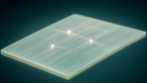
The Technical University of Denmark has demonstrated a high-purity single-photon emission device achieving a second-order correlation function of g(2)(0) = 0.003. The system utilizes a “van der Waals platform” that integrates strain-engineered bilayer WSe2 quantum emitters with multimode WS2 waveguides. The device recorded an out-coupled single-photon rate of approximately 357 kHz, which translates to an estimated on-chip generation rate of at least 1.68 MHz.
Technical Details
The architecture employs several specific material and design optimizations to enhance performance:
- Material Integration: Hexagonal boron nitride was used as a spacer during transfer to limit the fracturing of the WSe2 bilayer.
- Waveguide Configuration: Finite-difference time-domain models indicate that the use of multimode WS2 waveguides optimized light propagation and collection, contributing to the increased photon rates.
- Emission Control: Discrete-state excitation was used to minimize spectral background noise, resulting in brighter photoluminescence and higher purity.
- Measurement: Purity was verified through single-port and cross-correlated photon stream analysis. Confocal measurements of the emitter alone, prior to waveguide coupling, showed a g(2)(0) value of 0.043±0.027.
Background and Context
Current quantum photonic implementations typically rely on combining disparate material systems, such as silicon or silicon nitride for photonics, III-V semiconductors for emitters, and superconducting materials for detectors. This requires complex fabrication processes. The developed platform seeks to replace this with a monolithic integration of transition metal dichalcogenides (TMDs), where WSe2 serves as the emitter and WS2 provides low-loss photonic circuits including couplers and beam splitters.
Significance and Outlook
The ability to achieve MHz-level rates and high purity within a single material system represents a step toward scalable quantum communication networks. The researchers noted optimized transmittance between 750-850 nm with the grated structure, peaking around 800 nm. Future implementations aim for a fully integrated circuit incorporating niobium diselenide nanowires as fast single-photon detectors.
Source: https://quantumzeitgeist.com/technical-denmark-quantum-light-source-passes/
Get our weekly technology intelligence — free
Receive an infographic that lets you judge at a glance whether each field’s analysis report is worth reading.
Subscribe Free — Weekly Tech Intelligence
By subscribing, you’ll receive Troy-Technical’s weekly technology intelligence newsletter.
- Your email and selected fields are used only to deliver the newsletter.
- We never share your information with third parties.
- You can unsubscribe anytime via the link in each email.
See our Privacy Policy for details.
Takes about a minute · Unsubscribe anytime