


Key Findings
The developed AI SoC achieves a significant reduction in power consumption and boot latency by eliminating the need to transfer large volumes of data from external SSDs or DRAM upon power-up. System-level verification shows that a single frame inference using Tiny YOLOv3 requires 50.7mJ, which is 1/50th the energy of conventional methods. Additionally, the time from power-on to OS boot was reduced to 65.7 milliseconds, representing a 38.59-fold increase in speed.
Technical Details
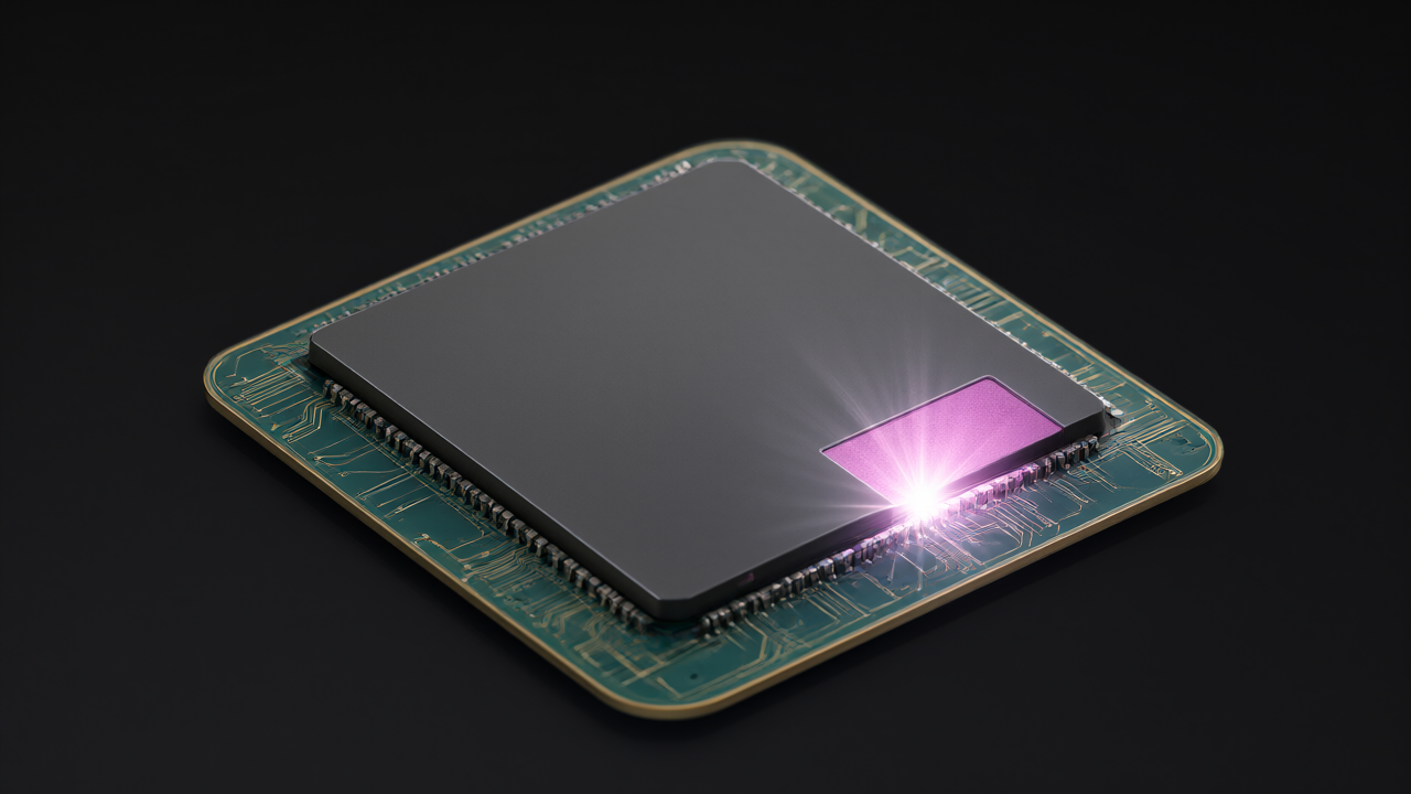
The chip is fabricated using TSMC’s 16nm FinFET process and integrates the following components on a single die:
- CPU: Dual-core Arm Cortex-A53
- GPU: Arm Mali-G31
- AI Accelerator: Tiny YOLOv3
- Non-volatile Memory: 32MB STT-MRAM
To optimize memory usage, the team implemented a hybrid multiplication architecture combining 8-bit and 16-bit precision and a weight-sharing technique. These innovations reduced the AI model weight data to 9.36MB, a 53% reduction compared to previous versions, while maintaining a mAP (mean Average Precision) of 0.316 (compared to 0.325). The weight-sharing technique further reduces data movement and local bandwidth by reusing weights within 4×4 tiles over multiple clock cycles.
Background and Context
Current edge AI systems face bottlenecks due to the increasing size of AI models, which necessitates massive data transfers between the processor and external memory. This leads to signal delays and increased power consumption. By integrating STT-MRAM directly on-chip, the research team—led by Professor Tetsuro Endo of the International Center for Integrated Electronics (CIES) at Tohoku University—allows the system to read weights directly from the non-volatile memory.
Significance and Outlook
The integration of CMOS and spintronics allows the SoC to perform AI processing in 58.5 milliseconds, compared to the previous 594.6 milliseconds, marking a 10-fold speed improvement. This capability enables high-speed object detection via Tiny YOLOv3 within limited memory constraints, providing a scalable solution for low-power, fast-booting edge AI applications in industrial and automotive sectors.
Source: https://eetimes.itmedia.co.jp/ee/articles/2611/05/news036.html
Get our weekly technology intelligence — free
Receive an infographic that lets you judge at a glance whether each field’s analysis report is worth reading.
Subscribe Free — Weekly Tech Intelligence
By subscribing, you’ll receive Troy-Technical’s weekly technology intelligence newsletter.
- Your email and selected fields are used only to deliver the newsletter.
- We never share your information with third parties.
- You can unsubscribe anytime via the link in each email.
See our Privacy Policy for details.
Takes about a minute · Unsubscribe anytime