Key Findings
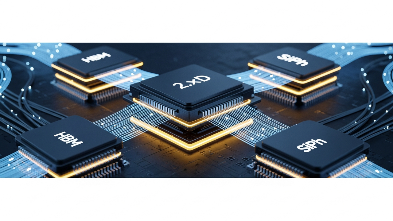
Samsung Electronics is developing a groundbreaking ‘2.xD’ advanced packaging technology that integrates high-bandwidth memory (HBM), logic chips, and silicon photonics (SiPh) into a single, cohesive package. This innovative solution is specifically designed to address the escalating power consumption and data transfer bottlenecks prevalent in modern AI data centers, promising a significant leap in AI system efficiency and performance.
Technical and Clinical Details
The ‘2.xD’ packaging leverages panel-based redistribution layer (RDL) interposers as its core, substantially enhancing wiring density and data transfer efficiency between HBM, logic, and SiPh chips. The bonding technology is also evolving from traditional micro bumps to bumpless hybrid bonding, enabling finer and more robust connections. Specifically, this technology aims to maximize inter-chip data transfer speeds and minimize power consumption for AI accelerators and server CPUs that demand extremely high bandwidth and low latency. Introduced at the Nano Korea 2026 forum, the successful implementation of this technology necessitates overcoming advanced manufacturing challenges such as fine particle control and substrate warpage, areas where Samsung is actively focusing its R&D efforts.
Background and Industry Context
The increasing complexity of AI models and the explosive growth in data volume have led to significant challenges in semiconductor chip performance limits and power consumption within data centers. Conventional packaging technologies often result in longer data transmission distances between chips, leading to unavoidable signal delays and power loss. Consequently, there is a surging demand for advanced packaging solutions that can physically bring together and more efficiently integrate chips with disparate functionalities, such as HBM, logic, and optical communication devices. Samsung benefits from a unique ‘triple-play’ portfolio comprising memory, foundry (logic), and silicon photonics, which allows for internal co-design and optimization of these diverse components.
Strategic Significance and Outlook
Samsung’s ‘2.xD’ packaging technology is poised to profoundly impact the design of next-generation AI computing infrastructure. By directly integrating HBM and logic chips with silicon photonics for optical data transmission, it becomes possible to create ultra-high-speed, low-power systems that transcend the limitations of electrical signals. This directly translates into reduced power consumption and a substantial increase in computational power for AI data centers, serving as a key accelerator for future AI advancements. Through this technology, Samsung aims to establish leadership in the AI packaging market, directly competing with co-packaged optics (CPO) technologies being jointly developed by NVIDIA and Broadcom with TSMC.
Source: https://www.digitimes.com/news/a20260713VL223/samsung-hbm-optics-siph-packaging-chips.html
Get our weekly technology intelligence — free
Receive an infographic that lets you judge at a glance whether each field’s analysis report is worth reading.
Subscribe Free — Weekly Tech Intelligence
By subscribing, you’ll receive Troy-Technical’s weekly technology intelligence newsletter.
- Your email and selected fields are used only to deliver the newsletter.
- We never share your information with third parties.
- You can unsubscribe anytime via the link in each email.
See our Privacy Policy for details.
Takes about a minute · Unsubscribe anytime









Comments