Key Findings
The evolution of AI chips is increasingly dependent on chiplet architectures and advanced packaging technologies, rather than solely transistor miniaturization, establishing a new growth driver for the semiconductor manufacturing equipment market. Applied Materials forecasts its revenue from advanced packaging to increase by over 50% in 2026, while KLA expects its advanced packaging portfolio to generate approximately $1 billion in revenue for the same year. Micron has announced plans to build end-to-end HBM (High Bandwidth Memory) packaging capabilities as part of its U.S. investment strategy.
Technical and Clinical Details
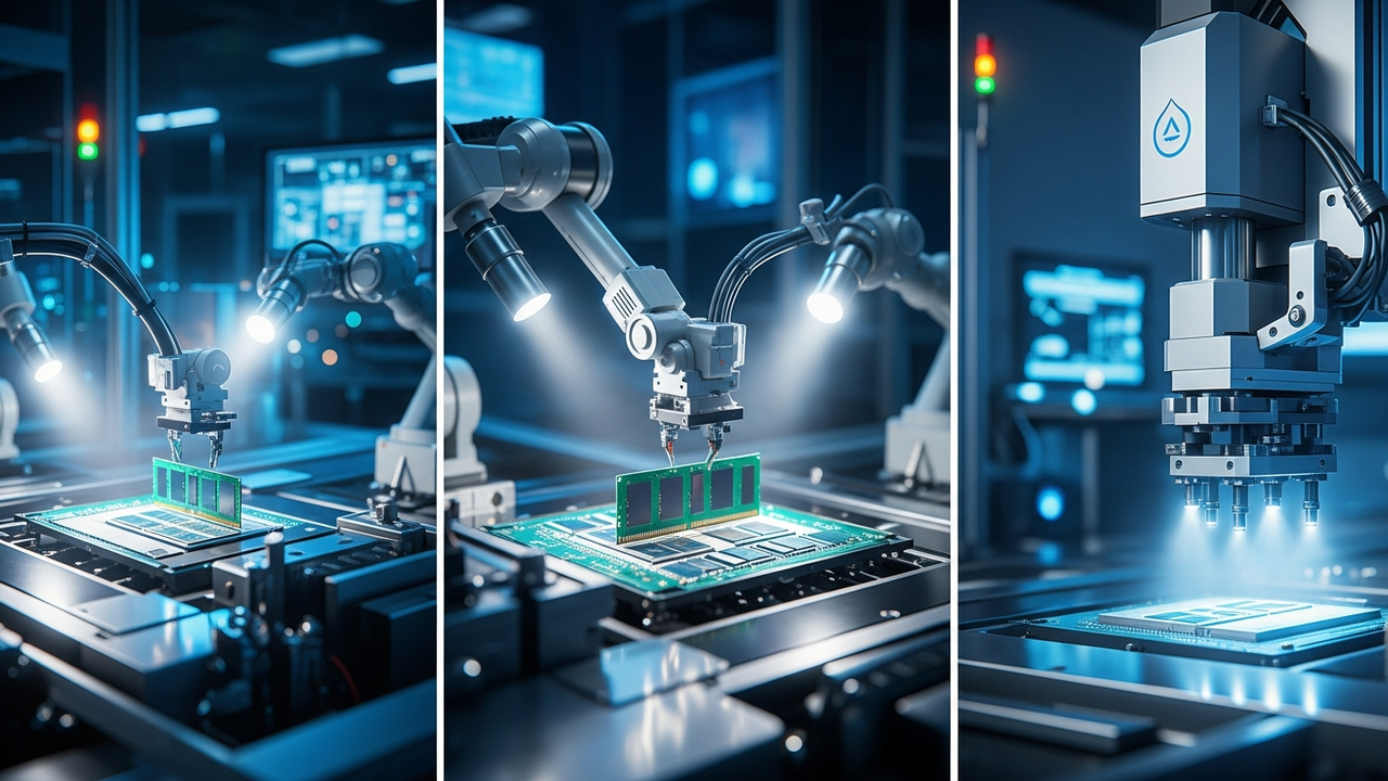
As AI chip designs become progressively complex, advanced packaging techniques, which integrate multiple functional blocks (chiplets) with high density within a single package, are becoming indispensable. This necessitates precise materials engineering and numerous processing steps, making equipment from providers like Applied Materials—covering etching, deposition, planarization, and inspection—extremely critical. Micron’s initiative to build end-to-end HBM packaging capability specifically involves integrating wafer bonding for HBM stack formation, wafer thinning for thermal management, advanced inspection for quality assurance, and precise material handling technologies. This comprehensive approach is expected to enhance HBM production yield and reliability, thereby maximizing the overall performance and efficiency of AI chips. KLA’s portfolio focuses on defect detection and metrology within the packaging process, contributing to manufacturing optimization.
Background and Industry Context
The explosive growth of AI has dramatically increased demand for computational power and bandwidth in data centers, exposing the limitations of traditional 2D chip designs. Technologies like HBM and chiplets were developed to overcome these challenges, and advanced packaging is key to their realization. Historically, semiconductor equipment investment focused primarily on front-end miniaturization. However, in the AI era, the importance of back-end packaging, testing, and material processing has risen to an equivalent, if not greater, level. The revenue forecasts from Applied Materials and KLA clearly reflect this market shift, indicating that semiconductor equipment manufacturers are becoming significant beneficiaries of the AI boom.
Strategic Significance and Outlook
The trend of AI chip performance evolution being deeply dependent on advanced packaging and materials engineering will persist. Equipment suppliers like Applied Materials and KLA are expected to capitalize on this structural change for long-term growth opportunities. Micron’s substantial investment in HBM packaging illustrates a strategy for memory manufacturers to capture AI-driven HBM demand and strengthen vertically integrated manufacturing capabilities. These developments signify an accelerating focus on back-end technologies within the overall semiconductor industry supply chain, serving as a powerful impetus for AI infrastructure development. Technological innovation and capital investment in this sector will be key to unlocking the potential of next-generation AI.
Get our weekly technology intelligence — free
Receive an infographic that lets you judge at a glance whether each field’s analysis report is worth reading.
Subscribe Free — Weekly Tech Intelligence
By subscribing, you’ll receive Troy-Technical’s weekly technology intelligence newsletter.
- Your email and selected fields are used only to deliver the newsletter.
- We never share your information with third parties.
- You can unsubscribe anytime via the link in each email.
See our Privacy Policy for details.
Takes about a minute · Unsubscribe anytime









Comments