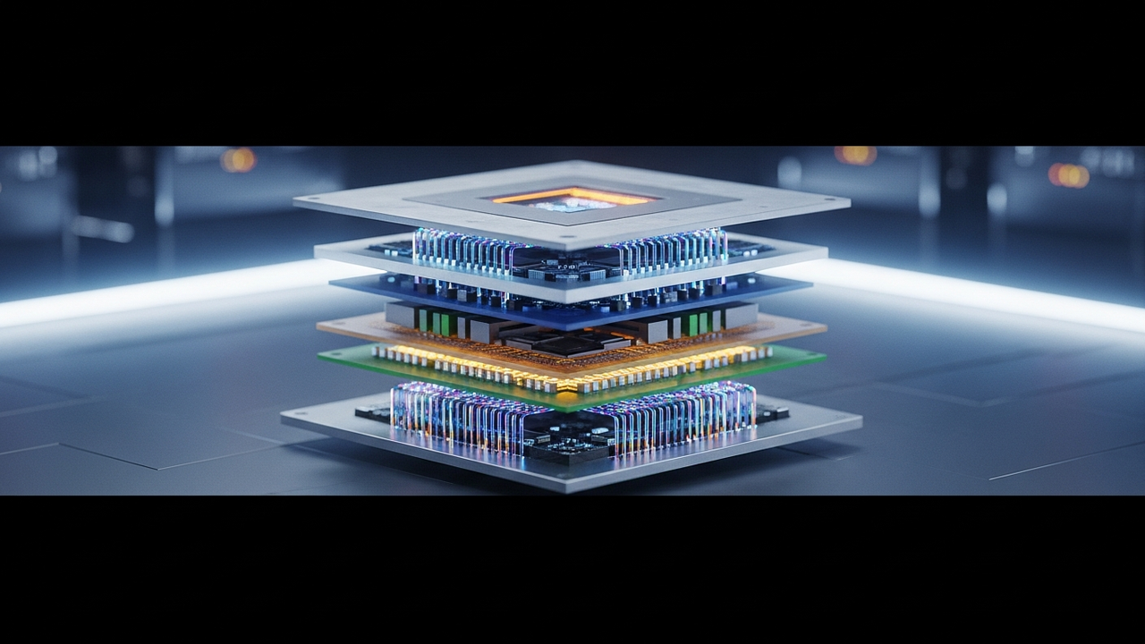
Key Findings: Samsung Tackles AI Power and Heat with “2.xD” Packaging
Samsung Electronics is aggressively pursuing the development of its groundbreaking “2.xD” next-generation packaging technology, designed to directly address the escalating power consumption and thermal management challenges faced by AI data centers. This innovative approach aims to integrate High Bandwidth Memory (HBM), high-performance logic chips, and silicon photonics (SiPh) into a single, advanced package.
Technical Details: Panel-Based RDL Interposers and Hybrid Bonding
- The “2.xD” packaging technology endeavors to surpass the limitations of conventional 2.5D packaging, which typically relies on silicon interposers. Samsung’s strategy involves adopting a larger, more cost-effective panel-based Redistribution Layer (RDL) interposer to seamlessly integrate HBM, logic chips, and SiPh components within the same package. This will dramatically increase data transfer density while minimizing inter-chip communication latency and energy consumption.
- Furthermore, Samsung is advancing the development of custom HBM solutions and hybrid bonding techniques. Custom HBM will offer memory performance optimized for specific AI workloads, while hybrid bonding is crucial for achieving ultra-high-density and efficient chip-to-chip connections, enhancing overall package performance and reliability. The convergence of these technologies is expected to significantly boost AI processor capabilities and substantially improve the operational efficiency of AI data centers.
Background & Industry Context: AI Data Centers’ New Bottlenecks
The proliferation of generative AI and large language models has led to an explosion in demand for AI data centers. However, this growth is increasingly constrained by physical bottlenecks: limitations in inter-chip data transfer speeds, massive power consumption, and the resulting excessive heat generation. Traditional packaging technologies are proving insufficient to meet these demands, necessitating new solutions that can more intimately integrate diverse components such as HBM, logic, and SiPh. Samsung’s “2.xD” stands as a direct response to these challenges, marking a significant step towards elevating AI chip performance to the next frontier.
Strategic Significance & Outlook: Driving AI Infrastructure Efficiency and Sustainability
The commercialization of “2.xD” packaging technology is poised to dramatically enhance the energy efficiency of AI data centers, contributing to reduced operational costs. Moreover, its high-speed, low-latency data transfer capabilities will enable the realization of more complex and larger-scale AI models, accelerating the further evolution of AI technology. The integration of silicon photonics, bringing optical communication to the package level, has the potential to break through the limits of electrical interconnections, enabling terabit-scale data transfer rates. This represents a pivotal advancement towards building sustainable AI infrastructure and is expected to further solidify Samsung’s leadership in the semiconductor industry.
Source: https://finance.biggo.com/news/92953789-b58b-4119-9c90-072ce5429b45
Get our weekly technology intelligence — free
Receive an infographic that lets you judge at a glance whether each field’s analysis report is worth reading.
Subscribe Free — Weekly Tech Intelligence
By subscribing, you’ll receive Troy-Technical’s weekly technology intelligence newsletter.
- Your email and selected fields are used only to deliver the newsletter.
- We never share your information with third parties.
- You can unsubscribe anytime via the link in each email.
See our Privacy Policy for details.
Takes about a minute · Unsubscribe anytime









Comments