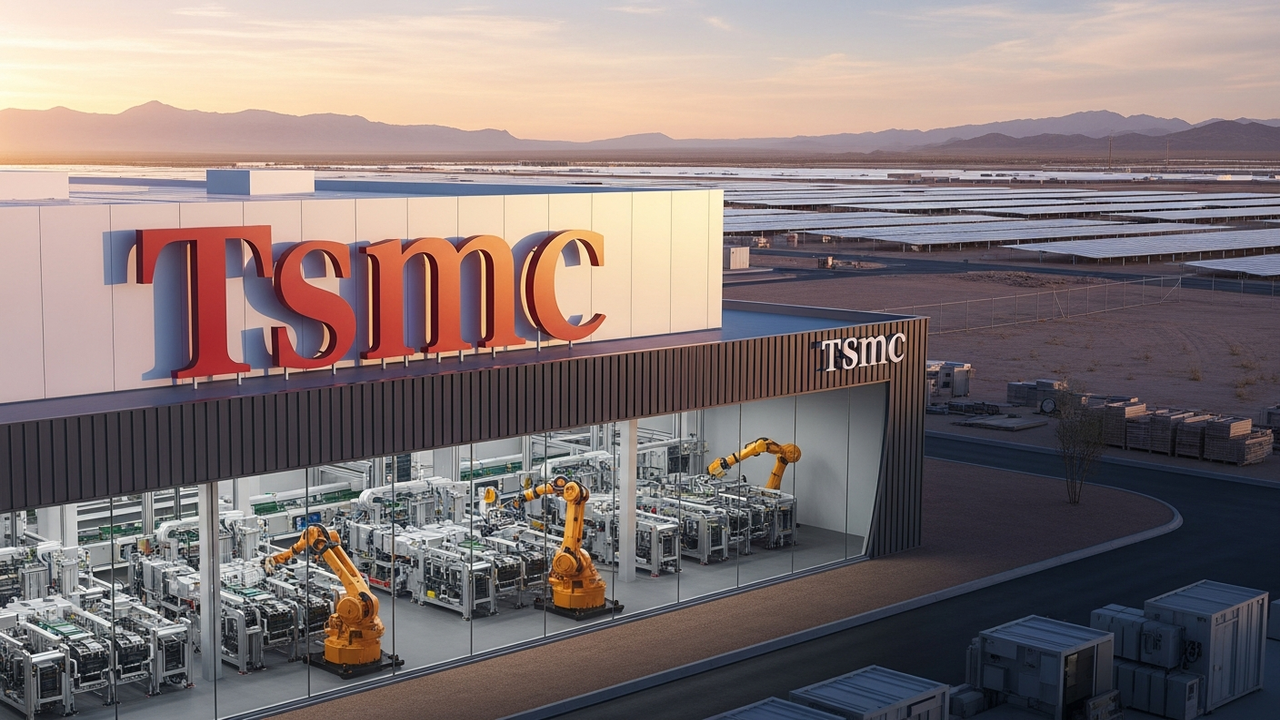
Key Findings: TSMC Pledges Additional $100 Billion for U.S. Semiconductor Manufacturing and Packaging, Totaling $265 Billion for 12 Facilities
TSMC, the world’s largest dedicated independent semiconductor foundry, has announced an additional $100 billion investment in advanced semiconductor manufacturing and packaging facilities in the United States. This commitment comes as part of a historic trade and investment agreement between the U.S. and Taiwan. With this new pledge, TSMC’s total investment in the U.S. will reach an unprecedented $265 billion, designated for the construction of 12 state-of-the-art semiconductor fabrication and packaging facilities across the country. This monumental investment is expected to dramatically reinforce U.S. domestic manufacturing capabilities, create tens of thousands of high-value jobs, and solidify America’s technological leadership for the future.
Technical & Business Details
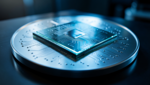
- Advanced Semiconductor Manufacturing and Packaging: The investment primarily targets cutting-edge logic chip manufacturing processes (e.g., 3nm and 2nm nodes) and advanced packaging solutions that enable High-Bandwidth Memory (HBM) and 2.5D/3D stacking technologies. These are indispensable components for next-generation technologies such as Artificial Intelligence (AI), High-Performance Computing (HPC), and advanced data centers.
- Job Creation and Economic Impact: TSMC anticipates that this colossal investment will generate tens of thousands of direct and indirect jobs. This includes construction workers, semiconductor manufacturing technicians, and R&D personnel, creating ripple effects across the entire related supply chain and revitalizing regional economies throughout the U.S.
- Strengthening U.S.-Taiwan Cooperation: The investment agreement is seen as further deepening the economic and strategic ties between the United States and Taiwan. Collaboration in the semiconductor supply chain is a mutual interest for both nations, increasingly vital for national security.
Background & Industry Context
The U.S. CHIPS and Science Act has provided substantial incentives to bolster domestic semiconductor manufacturing, driven by geopolitical risks and the vulnerabilities of past supply chains, leading the U.S. to strongly advocate for reshoring semiconductor production. The explosive growth of AI demand has further amplified the strategic importance of advanced semiconductor technology, attracting massive investments from global enterprises. TSMC’s commitment responds directly to these policy mandates and market demands.
Strategic Significance & Outlook
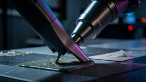
TSMC’s unparalleled investment is set to establish the U.S. as one of the world’s premier hubs for advanced semiconductor manufacturing and packaging. This will enhance the resilience and security of the global semiconductor supply chain, providing a robust foundation for the U.S. to assume a leading role in next-generation technological innovations, particularly in AI and HPC. This represents a decisive strategic move shaping the future of the global semiconductor industry. In the field of adhesives and sealants, the demand for high-reliability materials in these advanced packaging facilities will rapidly escalate.
Get our weekly technology intelligence — free
Receive an infographic that lets you judge at a glance whether each field’s analysis report is worth reading.
Subscribe Free — Weekly Tech Intelligence
By subscribing, you’ll receive Troy-Technical’s weekly technology intelligence newsletter.
- Your email and selected fields are used only to deliver the newsletter.
- We never share your information with third parties.
- You can unsubscribe anytime via the link in each email.
See our Privacy Policy for details.
Takes about a minute · Unsubscribe anytime




Comments