Key Findings
SK Hynix has reapproved a substantial additional investment of 7.1 trillion won (approximately $5.5 billion USD) for its P&T7 project in Cheongju, South Korea. This decision aims to significantly enhance the company’s advanced packaging capabilities for AI memory products, including High-Bandwidth Memory (HBM). This move underscores SK Hynix’s aggressive stance in responding to the rapid growth of the AI chip market.
Technical & Manufacturing Details
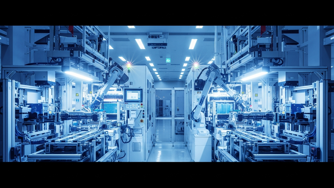
P&T7 will be SK Hynix’s seventh packaging and test facility. The factory will incorporate cutting-edge advanced packaging technologies essential for the production of HBM, a core component of AI accelerators. Specifically, state-of-the-art equipment and processes will be applied to critical stages such as chip stacking, micro-bump bonding, and wafer-level packaging (WLP). Construction of the facility began in April this year and is scheduled to proceed as follows:
- **Wafer Test Line Installation:** Expected to be completed by October 2027, enabling initial quality assurance for HBM and other memory dies.
- **Wafer-Level Packaging Line Construction:** Phased completion planned by February 2028. WLP is a key technology for producing AI memory, where miniaturization and high performance are paramount.
This extensive increase in production capacity is a direct response to the surging demand for memory specifically tailored for AI chips. HBM provides unparalleled bandwidth compared to conventional DRAM, making it an indispensable component for training and inference in AI models.
Background & Context
The rapid advancement of AI is driving structural changes in the global semiconductor industry, leading to an explosive increase in demand for high-performance AI chips and their associated memory. Major AI chip manufacturers, such as Nvidia, are actively strengthening their collaborations with memory suppliers to secure a stable supply of HBM. SK Hynix is one of the world’s leading HBM suppliers, and this latest investment holds strategic significance in further solidifying its competitive advantage. Amidst the ongoing reconfiguration of global supply chains, strengthening domestic advanced packaging capabilities is also crucial from the perspectives of technological self-reliance and economic security.
Strategic Significance & Outlook
SK Hynix’s substantial investment in P&T7 will significantly boost its supply capacity in the HBM and AI memory markets, contributing to the alleviation of AI chip supply bottlenecks. This is expected to accelerate the further development and widespread adoption of AI technologies. However, with competitors like Samsung and Micron also aggressively expanding their HBM production capacities, competition for market share and technological leadership is expected to intensify. The full operation of P&T7 will serve as a critical foundation for SK Hynix to play a central role in the AI era’s semiconductor market. Additionally, advancements in peripheral technologies, such as cooling solutions, will be key to future competition in maximizing HBM performance.
Source: https://www.thelec.net/news/articleView.html?idxno=12449
Get our weekly technology intelligence — free
Receive an infographic that lets you judge at a glance whether each field’s analysis report is worth reading.
Subscribe Free — Weekly Tech Intelligence
By subscribing, you’ll receive Troy-Technical’s weekly technology intelligence newsletter.
- Your email and selected fields are used only to deliver the newsletter.
- We never share your information with third parties.
- You can unsubscribe anytime via the link in each email.
See our Privacy Policy for details.
Takes about a minute · Unsubscribe anytime









Comments