Key Findings
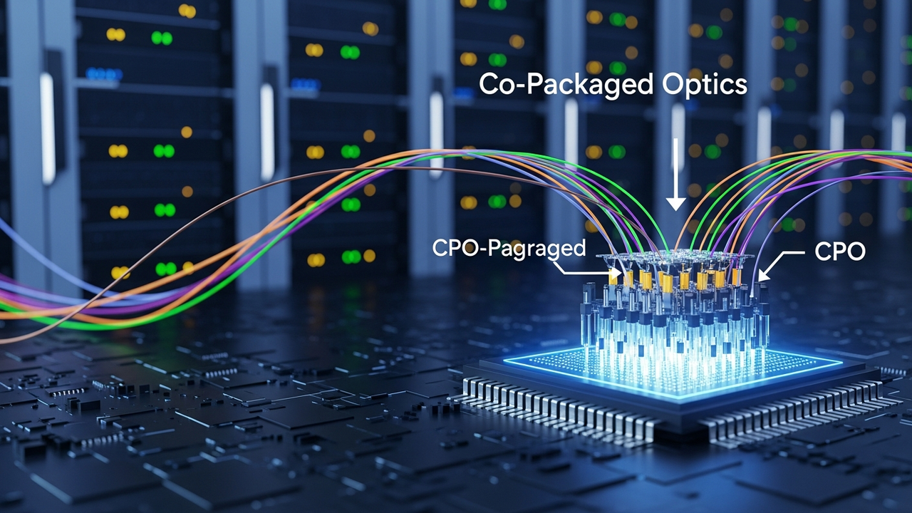
The escalating demand for Co-Packaged Optics (CPO) is fundamentally reshaping the priorities of semiconductor manufacturing within both advanced packaging and AI processor supply chains. CPO is rapidly transitioning from a phase of technological development to full-scale commercial deployment, serving as a critical enabler for the higher bandwidth and significant power consumption reductions required by advanced AI clusters.
Technical & Application Details
CPO involves integrating optical transceivers, which convert electrical signals into optical signals, directly within the same package as the data-processing semiconductor chips (ASICs or GPUs). This integration dramatically shortens the electrical wiring distance between the chip and external devices, substantially reducing signal loss. The result is ultra-high-speed data transmission and significant power savings. Particularly in AI data centers, where terabit-scale data transfer rates and improved performance-per-watt are essential due to the expanding scale of AI workloads, CPO is being recognized as an ideal solution.
Implementing CPO requires highly advanced technologies and manufacturing capabilities, including:
- **Additional Wafer Processing:** Specialized wafer-level processing to integrate optical components with semiconductor processes.
- **Precision Assembly Techniques:** High-precision assembly to integrate optical and electronic components with sub-millimeter accuracy.
- **Advanced Packaging Capabilities:** Complex packaging techniques to incorporate optical components on top of existing advanced packaging foundations that already integrate high-performance processors and HBM (High-Bandwidth Memory).
These stringent requirements are expected to further intensify competition for already limited advanced packaging resources, such as CoWoS.
Background & Context
The rapid evolution of AI places unprecedented demands on computing power and network bandwidth within data centers. Conventional copper-based electrical interconnects are encountering physical limitations, primarily increasing signal loss and power consumption as speeds rise. CPO is anticipated to break through this ‘electrical wall,’ dramatically improving data transmission efficiency between AI chips and network infrastructure. Leading cloud providers and AI hardware vendors are actively exploring CPO as an indispensable component for next-generation AI infrastructure, a factor that is reshaping strategic priorities across the entire semiconductor supply chain.
Strategic Significance & Outlook
The commercial deployment of CPO is expected to elevate AI chip performance and energy efficiency to new levels, enabling further breakthroughs in AI technology. However, its realization necessitates close collaboration among semiconductor manufacturers, OSAT companies, and optical component suppliers, along with continuous investment in advanced packaging technologies. Overcoming the challenges of CPO standardization and mass production amidst intensifying competition for limited resources will be key to its widespread adoption. In the long term, CPO is expected to fundamentally transform AI data center architectures, contributing to the construction of more sustainable and high-performance AI infrastructures.
Get our weekly technology intelligence — free
Receive an infographic that lets you judge at a glance whether each field’s analysis report is worth reading.
Subscribe Free — Weekly Tech Intelligence
By subscribing, you’ll receive Troy-Technical’s weekly technology intelligence newsletter.
- Your email and selected fields are used only to deliver the newsletter.
- We never share your information with third parties.
- You can unsubscribe anytime via the link in each email.
See our Privacy Policy for details.
Takes about a minute · Unsubscribe anytime









Comments