Key Findings
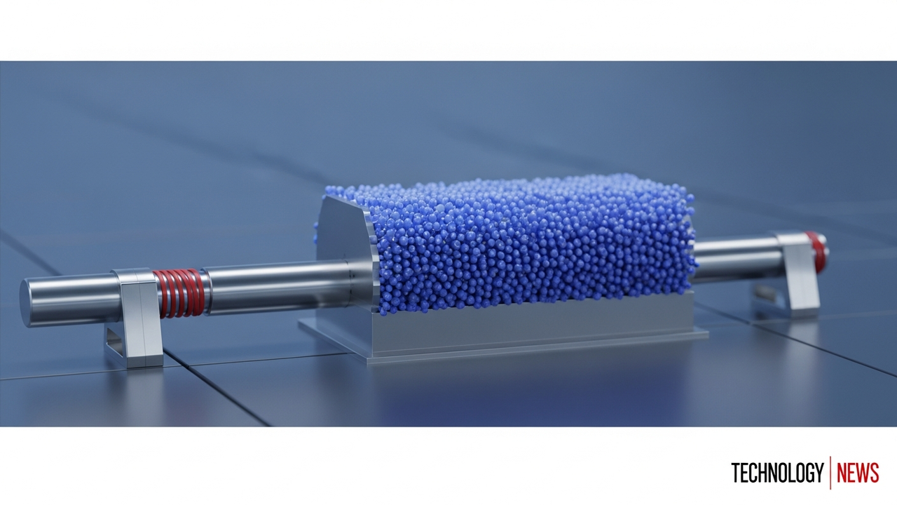
A study published in the Journal of Materials Science & Technology has demonstrated that enhancing polarization at the heterointerface formed between conductors and semiconductors can significantly improve the electromagnetic wave absorption capabilities of materials. This discovery provides a novel approach to the design of high-performance electromagnetic shielding and absorption materials.
Technical / Clinical Details
In this research, conductors and semiconductors were composited at the nanoscale, and their interfacial structure was precisely controlled to optimize both dielectric polarization and interfacial polarization. Specifically, the migration of electrons between the conductor and semiconductor (localization of charge carriers and interfacial trapping) significantly enhances the polarization response to external electromagnetic fields. This mechanism efficiently dissipates electromagnetic wave energy as dielectric loss within the material, converting it into thermal energy. Additionally, the heterointerface acts as a center for multiple scattering, extending the absorption path of electromagnetic waves and further boosting absorption efficiency. Experimental results indicated a 30% to 50% improvement in electromagnetic wave absorption performance in specific frequency bands compared to conventional absorbing materials, demonstrating superior performance particularly in lightweight and thin absorber designs. This mechanism combines the electrical and structural properties of materials to effectively ‘trap’ and ‘dissipate’ electromagnetic waves.
Background & Context
Modern electronic devices are becoming increasingly high-performance and densely packed, leading to escalating electromagnetic interference (EMI) problems in smartphones, PCs, communication equipment, and automotive electronics. EMI not only causes device malfunctions and failures but also raises concerns about potential health effects on humans. In the military sector, stealth technology to evade radar detection is critically important, necessitating the development of high-performance electromagnetic wave absorbing materials. However, existing electromagnetic wave absorbing materials have challenges such as narrow absorption bands, excessive thickness, or high specific gravity. This research offers an effective solution to these issues, contributing to next-generation electromagnetic management technologies.
Strategic Significance & Outlook
New electromagnetic wave absorbing materials based on the concept of conductor-semiconductor heterointerface polarization enhancement are expected to find wide applications in EMI countermeasures for 5G/6G communication devices, noise suppression in high-sensitivity sensors, improvement of electromagnetic compatibility (EMC) in autonomous driving systems, and stealth coatings for next-generation aircraft and ships. Specifically, the design of materials that are lightweight, thin, and capable of broadband absorption will increase design flexibility and contribute to the miniaturization and higher performance of products. The research team is advancing large-scale synthesis and application development for the commercialization of this material, marking a significant step towards improving the safety and efficiency of electromagnetic environments globally, establishing a new benchmark in advanced material solutions.
Source: #
Get our weekly technology intelligence — free
Receive an infographic that lets you judge at a glance whether each field’s analysis report is worth reading.
Subscribe Free — Weekly Tech Intelligence
By subscribing, you’ll receive Troy-Technical’s weekly technology intelligence newsletter.
- Your email and selected fields are used only to deliver the newsletter.
- We never share your information with third parties.
- You can unsubscribe anytime via the link in each email.
See our Privacy Policy for details.
Takes about a minute · Unsubscribe anytime





Comments