Key Findings
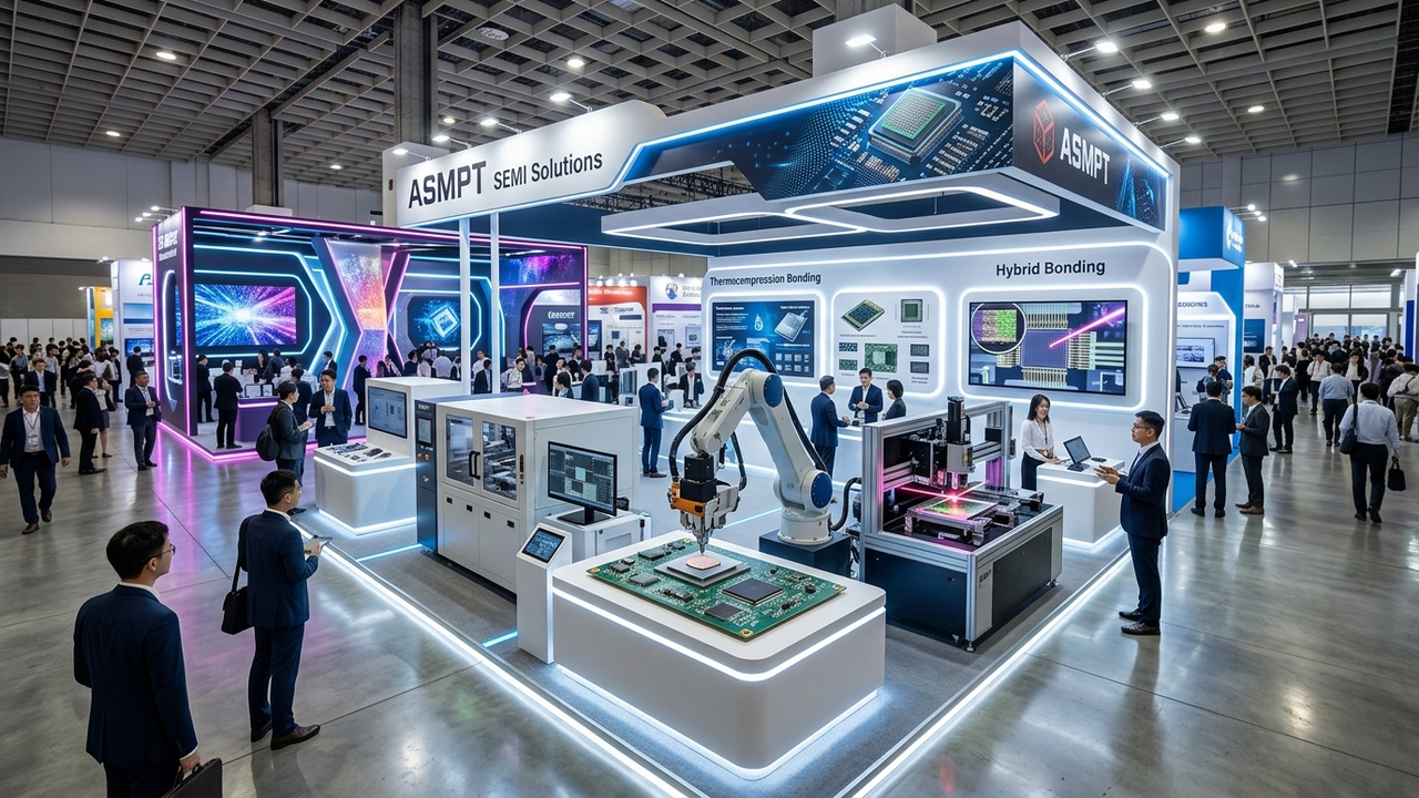
ASMPT, a global technology leader, announced its plan to showcase groundbreaking advanced packaging technologies at SEMICON Taiwan in September 2026. These innovations are designed to robustly support cutting-edge applications such as High-Performance Computing (HPC), AI accelerators, silicon photonics, and Co-Packaged Optics (CPO). The company will feature its expertise in critical techniques like Thermocompression Bonding (TCB) and Hybrid Bonding, presenting solutions that enable high-precision chiplet integration and high-speed data transfer. This exhibition underscores ASMPT’s technological leadership in meeting the complex semiconductor packaging demands of the AI era.
Technical Details
Central to ASMPT’s exhibit will be its MEGA multi-chip bonding solution, a system renowned for its exceptional chip placement and alignment accuracy. This solution integrates sophisticated dispensing, UV curing, and advanced inspection capabilities, facilitating ultra-fine pitch bonding essential for efficiently and reliably integrating numerous chiplets. Thermocompression Bonding (TCB) enables fine-pitch copper-to-copper interconnections, delivering high electrical performance and superior thermal management when combined with low coefficient of thermal expansion (CTE) materials. Hybrid bonding, offering even finer connection pitches and higher bond strengths, is a pivotal technology for die-to-wafer or die-to-die connections in 3D-ICs, crucial for next-generation chiplet architectures. These technologies collectively drive significant improvements in performance and power efficiency, particularly for AI processing units and High Bandwidth Memory (HBM) modules in data centers.
Background and Industry Context
The semiconductor industry faces unprecedented demands for speed, miniaturization, and higher integration driven by megatrends like AI, 5G, and autonomous driving. As the limits of traditional transistor scaling become apparent, heterogeneous integration—the strategy of segmenting functionalities into chiplets and integrating them using advanced packaging—has emerged as a vital path forward. Taiwan stands as a global hub for the semiconductor supply chain, and SEMICON Taiwan is one of the most significant semiconductor events in the Asia-Pacific region. Major suppliers like ASMPT unveiling their latest technologies here significantly impacts the entire semiconductor ecosystem in Taiwan and globally.
Strategic Significance and Outlook
ASMPT’s advanced packaging technologies are poised to play an indispensable role in semiconductor manufacturing for the AI era. High-density chiplet integration and low-latency data transfer are paramount for achieving peak performance in HPC and AI accelerators. The company’s solutions not only meet these immediate requirements but also pave the way for future technological frontiers such as Co-Packaged Optics (CPO). CPO, which integrates optical and electronic devices within a single package, promises to revolutionize data transfer by eliminating bottlenecks and drastically reducing power consumption in data centers, while boosting performance. ASMPT’s continuous innovation is set to shape the future of semiconductor packaging and accelerate the evolution of digital society.
Get our weekly technology intelligence — free
Receive an infographic that lets you judge at a glance whether each field’s analysis report is worth reading.
Subscribe Free — Weekly Tech Intelligence
By subscribing, you’ll receive Troy-Technical’s weekly technology intelligence newsletter.
- Your email and selected fields are used only to deliver the newsletter.
- We never share your information with third parties.
- You can unsubscribe anytime via the link in each email.
See our Privacy Policy for details.
Takes about a minute · Unsubscribe anytime









Comments