Key Findings
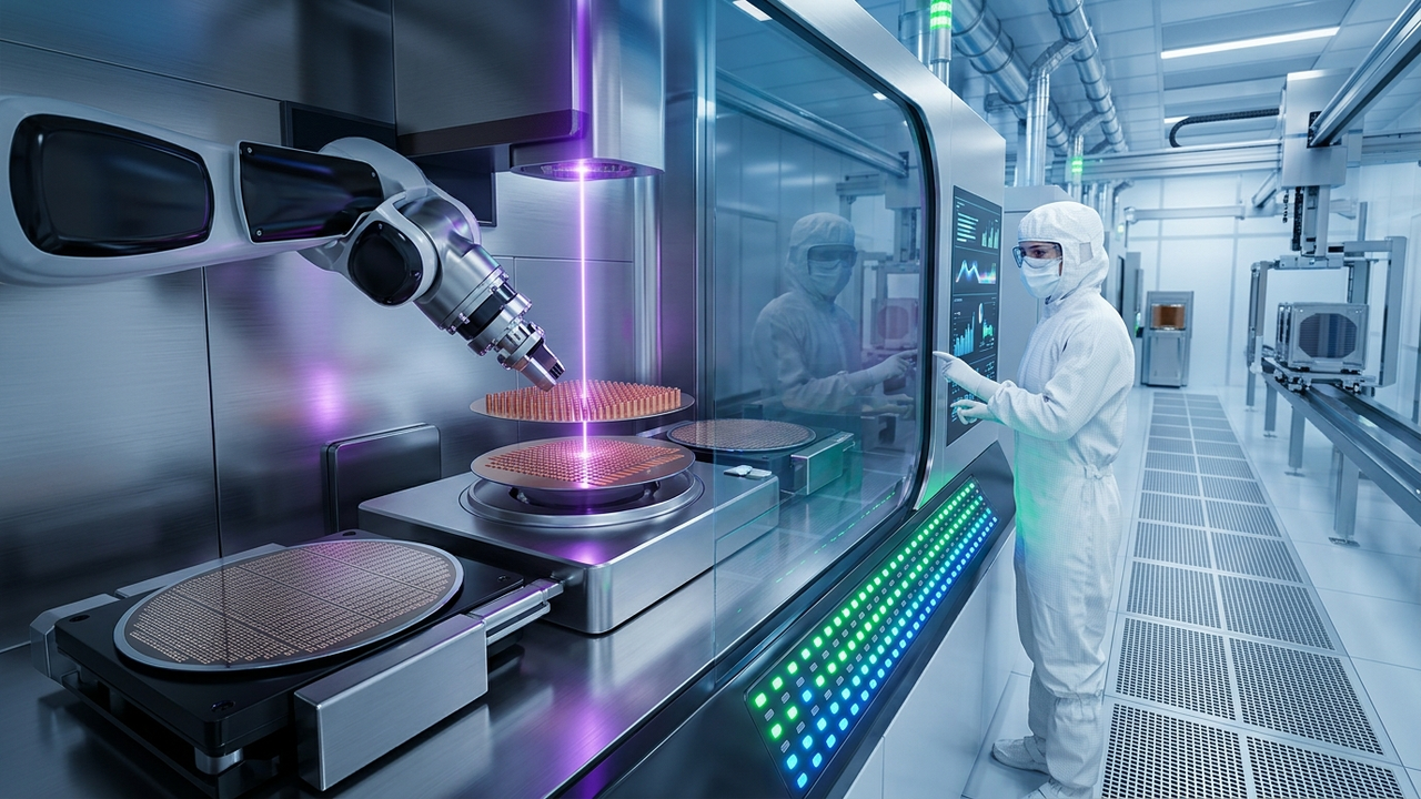
Applied Materials has unveiled a new hybrid bonding platform aimed at enabling the mass production of 3D stacked chips, which are essential for realizing next-generation high-performance semiconductors. This state-of-the-art system achieves ultra-fine pitch, high-precision alignment, and high throughput simultaneously in hybrid bonding—a technology that directly joins chips to chips or chips to wafers at a molecular level, surpassing conventional limitations. Hybrid bonding plays a decisive role in enhancing performance and power efficiency for AI (Artificial Intelligence) and HPC (High-Performance Computing) chips by significantly increasing connection density and shortening signal transmission distances compared to traditional micro-bump connections. This new platform from Applied Materials represents a major step towards the commercial mass production of a technology previously in R&D, marking a crucial breakthrough that will accelerate the adoption of 3D-ICs (3D Integrated Circuits).
Technical and Platform Details
The main features and technical advantages of the new platform include:
- Ultra-Fine Pitch Capability: Enables hybrid bonding at extremely fine connection pitches, below several microns, leading to higher density stacking.
- High-Precision Alignment: Advanced optical systems and control technologies achieve sub-micron level alignment accuracy for multiple chips, minimizing bonding defects.
- High Throughput: Integrates high-speed handling and bonding processes, optimizing productivity for mass production lines.
- Process Integration and Yield Improvement: Optimizes the entire process chain from pre-bonding treatment to bonding and final inspection, contributing to overall yield enhancement.
- Flexible Compatibility: Supports both die-to-wafer (D2W) and wafer-to-wafer (W2W) hybrid bonding methods.
This platform is expected to be applied across various advanced packaging applications, including next-generation HBM (High Bandwidth Memory) stacks, chiplet interconnections, and 3D-SoCs (System-on-Chips).
Background and Industry Context
As semiconductor miniaturization faces the limits of Moore’s Law, chiplet technology and 3D stacking have emerged as new frontiers for improving semiconductor performance and cost efficiency. Hybrid bonding is a foundational technology for enabling these advancements, indispensable for resolving power consumption, heat generation, and data transmission speed challenges in AI chips. As a leading semiconductor equipment manufacturer, Applied Materials is playing a critical role in alleviating this bottleneck, thereby accelerating innovation across the entire industry.
Strategic Significance and Outlook
Applied Materials plans to deploy this new platform to major semiconductor manufacturers and OSATs (Outsourced Semiconductor Assembly and Test providers), actively supporting the mass production adoption of 3D stacked chips. Looking ahead, the company aims to apply this technology to more complex heterogeneous integration and next-generation technologies like optoelectronic convergence, continuing to lead the evolution of semiconductor packaging technology. This technology will serve as a fundamental pillar supporting data-centric future societies, including AI, HPC, 5G/6G communication, and autonomous driving.
Source: #
Get our weekly technology intelligence — free
Receive an infographic that lets you judge at a glance whether each field’s analysis report is worth reading.
Subscribe Free — Weekly Tech Intelligence
By subscribing, you’ll receive Troy-Technical’s weekly technology intelligence newsletter.
- Your email and selected fields are used only to deliver the newsletter.
- We never share your information with third parties.
- You can unsubscribe anytime via the link in each email.
See our Privacy Policy for details.
Takes about a minute · Unsubscribe anytime









Comments