Key Findings
The rapid advancements in Artificial Intelligence (AI) technology are catalyzing a significant transformation in semiconductor packaging, giving rise to a new paradigm that extends beyond the physical limitations of traditional silicon interposers. Specifically, panel-based packaging is emerging as a pivotal solution to address the challenges posed by increasingly larger form factors and novel substrate materials.
Technical / Clinical Details
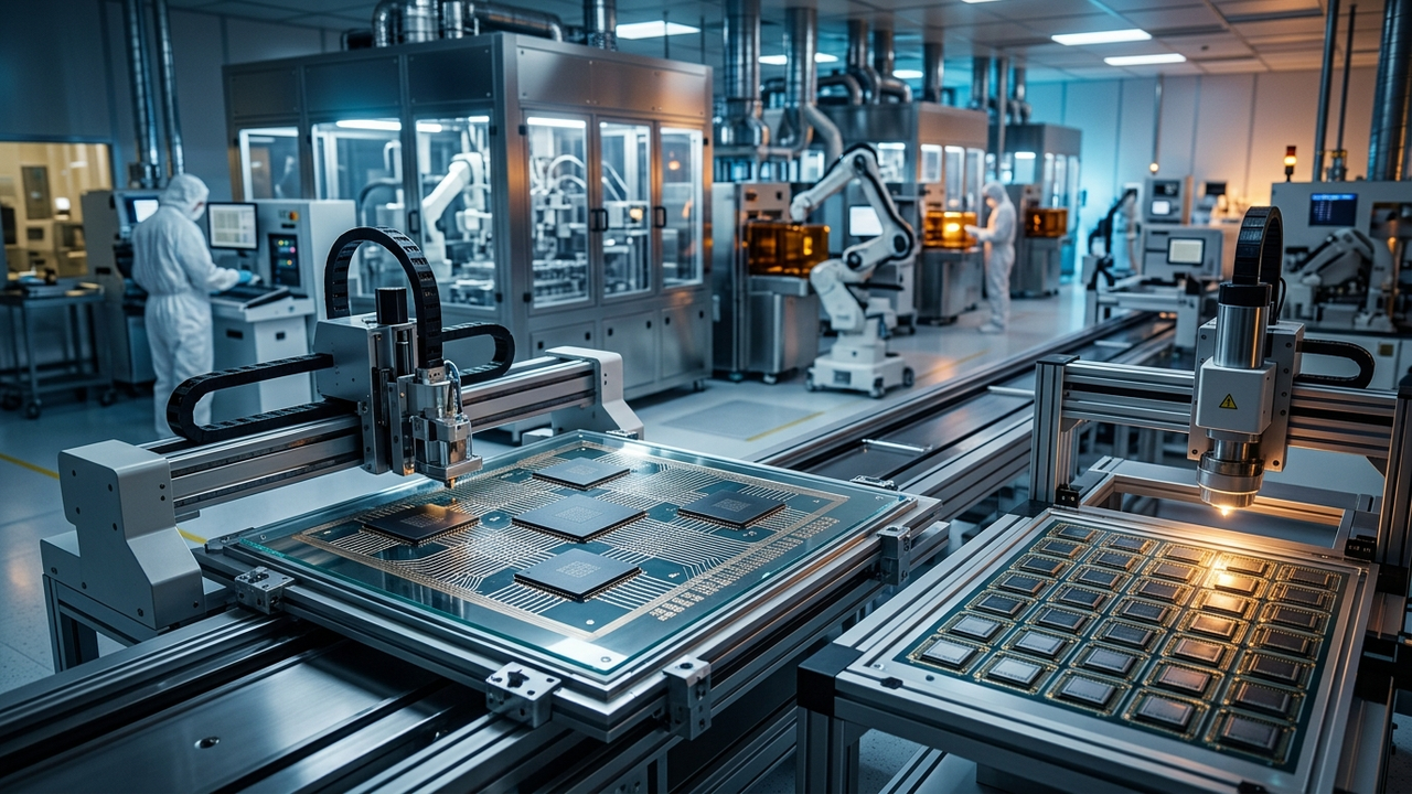
The performance requirements of AI applications are leading to an increase in the size and complexity of individual chips, alongside a growing need to integrate multiple components, such as High Bandwidth Memory (HBM). This demands larger package sizes that conventional wafer-based packaging technologies cannot effectively accommodate. Panel-based packaging involves processing multiple chips simultaneously on large square or rectangular panels, offering the potential to enhance production efficiency and reduce manufacturing costs. This technology is intimately linked with the evolution of fan-out packaging (FOPLP) and plays a crucial role in bridging the size gap between chips and motherboards. Specifically, achieving finer Redistribution Layers (RDLs) and higher throughput, in conjunction with advancements in technologies like Wafer-Level Chip Scale Package (WLCSP) and Through Silicon Via (TSV), is imperative for the success of packaging destined for AI and High-Performance Computing (HPC).
Background & Context
As the semiconductor industry grapples with the perceived limits of Moore’s Law, focus has shifted from solely improving internal chip performance to optimizing system-level performance through packaging technologies. The intensification of AI processors and HBM has particularly complicated packaging challenges related to thermal management, power delivery, and signal integrity. While traditional silicon interposers have been adopted primarily for niche high-performance applications due to cost and size constraints, the widespread adoption of AI necessitates more versatile and economically scalable packaging solutions. In this context, panel-based packaging is positioned as a significant innovation for next-generation semiconductor manufacturing.
Strategic Significance & Outlook
The progression of panel-based packaging technology is poised to be a crucial driver for further accelerating the growth of the AI and HPC markets. This will enable the realization of higher-performance and more cost-effective AI chips, facilitating the broader adoption of AI across various applications, including data centers, edge AI devices, and autonomous vehicles. The success of this new technology mandates continuous innovation in materials science, manufacturing equipment, and process technologies, requiring collaborative efforts across the industry. In the future, panel-based packaging has the potential to become a mainstream semiconductor packaging technology, serving as a core foundation for the computing infrastructure of the AI era.
Get our weekly technology intelligence — free
Receive an infographic that lets you judge at a glance whether each field’s analysis report is worth reading.
Subscribe Free — Weekly Tech Intelligence
By subscribing, you’ll receive Troy-Technical’s weekly technology intelligence newsletter.
- Your email and selected fields are used only to deliver the newsletter.
- We never share your information with third parties.
- You can unsubscribe anytime via the link in each email.
See our Privacy Policy for details.
Takes about a minute · Unsubscribe anytime







Comments