Key Findings
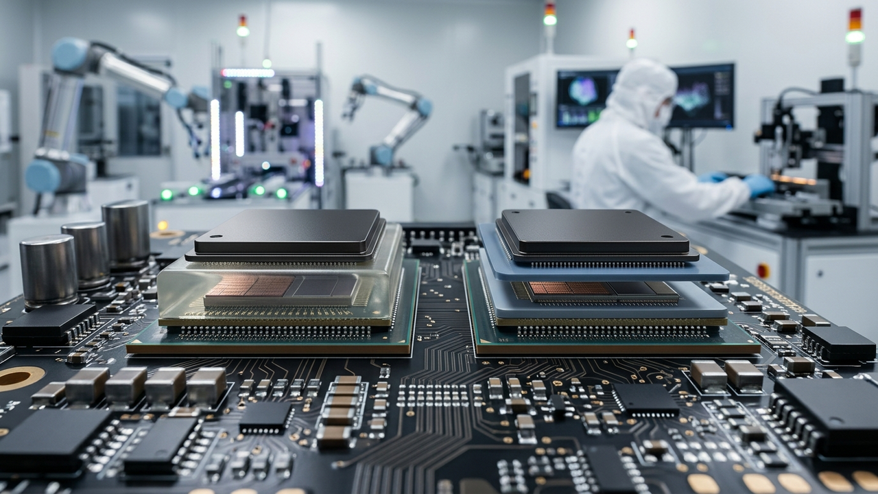
The rapid advancement of AI is instigating unprecedented evolution in semiconductor packaging, particularly for High Bandwidth Memory (HBM) technology. SK hynix’s Advanced Mass Reflow Molded Underfill (MR-MUF) technology and Samsung’s Thermal Compression Non-Conductive Film (TC-NCF) technology are resolving pressing thermal management and warpage issues associated with increased HBM density, thereby dramatically improving the performance and reliability of AI semiconductors.
Technical / Clinical Details
SK hynix’s Advanced MR-MUF technology significantly improves heat dissipation in HBM stacks. In this process, a liquid epoxy molding compound is precisely filled between micro-bumps, minimizing voids. This novel epoxy molding compound exhibits excellent thermal conductivity, especially in 16-high HBM4 configurations, efficiently channeling heat from the chips to the heat sink. This prevents performance degradation due to overheating and extends chip lifespan. Meanwhile, Samsung’s TC-NCF technology was developed to accommodate thinner dies and narrower gaps. NCF is a non-conductive film that melts during the thermal compression (TC) bonding process, uniformly filling the extremely fine gaps between chips. This effectively manages warpage issues and enables precise stacking of multiple dies. Both companies’ technologies are indispensable for ensuring high yield and reliability in increasingly complex heterogeneous integration.
Background & Context
The surge in AI demand is pushing the boundaries of data processing capabilities, compelling semiconductor manufacturers to develop high-performance, high-integration, and efficient thermal management solutions. As evidenced by Intel’s advanced packaging strategies and TSMC’s CoWoS™ architecture roadmap, increasing package dimensions are an unavoidable trend. HBM is a key memory technology for maximizing the performance of AI processors, but its multi-layer stacking structure creates thermal challenges and mechanical stresses that conventional packaging technologies struggle to address. SK hynix and Samsung are proactively tackling these issues by developing their respective unique materials and process technologies. This represents a strategic investment to establish competitive advantage in the AI-driven semiconductor market, highlighting the crucial role of materials science and process engineering convergence.
Strategic Significance & Outlook
SK hynix’s MR-MUF and Samsung’s TC-NCF technologies will play pivotal roles in shaping the future of AI semiconductors and HBM. These innovations will enable faster, more powerful, and more reliable AI systems, accelerating the adoption of AI in a wide range of applications such as data centers, autonomous driving, and edge AI devices. Moving forward, both companies are expected to continuously evolve these technologies to support further high-stacking of next-generation HBM (HBM4 and beyond) and more complex heterogeneous integration. Close collaboration with material suppliers and the optimization and automation of manufacturing processes will be key to the success of these technologies, driving the overall technological roadmap of the semiconductor industry.
Source: https://www.usdanalytics.com/our-insights/chemicals/ai-semiconductor-packaging-advanced-materials-1
Get our weekly technology intelligence — free
Receive an infographic that lets you judge at a glance whether each field’s analysis report is worth reading.
Subscribe Free — Weekly Tech Intelligence
By subscribing, you’ll receive Troy-Technical’s weekly technology intelligence newsletter.
- Your email and selected fields are used only to deliver the newsletter.
- We never share your information with third parties.
- You can unsubscribe anytime via the link in each email.
See our Privacy Policy for details.
Takes about a minute · Unsubscribe anytime






Comments