
Background
The relentless pursuit of miniaturization and enhanced performance, primarily driven by Moore’s Law, continues to define the semiconductor industry. While extreme ultraviolet (EUV) lithography currently represents the cutting edge for advanced node manufacturing, its prohibitive capital investment and operational costs restrict its accessibility for many manufacturers. In this context, alternative technologies like Nanoimprint Lithography (NIL) offer a promising avenue to democratize advanced semiconductor manufacturing, enabling a wider array of companies to participate in leading-edge logic processes. DNP’s latest innovation in NIL holds significant potential to bolster the global supply of high-performance semiconductors essential for diverse applications, including data centers, artificial intelligence (AI) processors, and Internet of Things (IoT) devices.
Key Findings
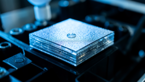
Dai Nippon Printing (DNP) has announced a pivotal breakthrough in semiconductor manufacturing with the development of a 10nm linewidth nanoimprint lithography (NIL) template, specifically engineered for 1.4nm-class logic semiconductors. This innovative technology delivers comparable 10nm-level patterning precision at approximately one-tenth the energy consumption of conventional extreme ultraviolet (EUV) lithography. DNP projects mass production to commence by 2027, with a strategic goal to generate 4 billion JPY in sales from this technology by fiscal year 2030.
Technical Details
Nanoimprint lithography (NIL) fundamentally differs from light-based exposure methods by physically stamping patterns onto a substrate. This ‘imprinting’ process eliminates the need for complex, costly optical systems found in EUV, leading to significantly simpler equipment designs and substantial energy savings. DNP’s newly developed 10nm template is crucial for accurately transferring ultra-fine circuit patterns, a requirement for 1.4nm generation semiconductors where the miniaturization of gate length and wiring width directly dictates performance improvements. Unlike EUV lithography, which demands massive capital expenditure and high operational outlays, NIL presents a more cost-effective alternative, potentially making advanced logic processes more accessible to semiconductor manufacturers without extensive EUV infrastructure.
Strategic Significance and Outlook
DNP’s commitment to initiating mass production of this 10nm NIL technology by 2027 signals its intent to establish a new manufacturing paradigm within the semiconductor industry. The ambitious sales target of 4 billion JPY by fiscal year 2030 reflects the company’s strong confidence in the commercial viability and market adoption of this technology. Beyond its economic potential, NIL technology carries significant strategic value, particularly in light of the monopolistic control over EUV scanner supply and prevailing geopolitical risks, offering a pathway to diversify the critical semiconductor supply chain. Looking ahead, this technology is poised to enable the cost-effective manufacturing of next-generation semiconductors, thereby supporting the continuous evolution and expansion of AI and high-performance computing capabilities.
Get our weekly technology intelligence — free
Receive an infographic that lets you judge at a glance whether each field’s analysis report is worth reading.
Subscribe Free — Weekly Tech Intelligence
By subscribing, you’ll receive Troy-Technical’s weekly technology intelligence newsletter.
- Your email and selected fields are used only to deliver the newsletter.
- We never share your information with third parties.
- You can unsubscribe anytime via the link in each email.
See our Privacy Policy for details.
Takes about a minute · Unsubscribe anytime








Comments