Key Findings
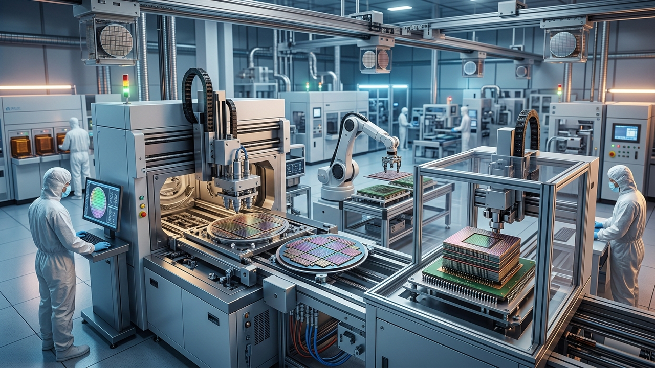
Applied Materials has unveiled new Chemical Mechanical Planarization (CMP), Electrochemical Deposition (ECD), deposition, and e-beam systems specifically designed for High Bandwidth Memory (HBM) and 3D packaging, in response to the massive scaling requirements of AI computing. Concurrently, the company has strategically acquired ASMPT’s NEXX business to further bolster its advanced packaging capabilities. Applied Materials anticipates its advanced packaging business to grow by over 50% in 2026, driven by the vision of next-generation packages potentially integrating over 300 chips, 500 billion transistors, and more than 2,000 miles of wiring.
Technical & Clinical Details
The newly launched systems by Applied Materials address the intricate demands of HBM stacking, chiplet integration, and advanced interconnects crucial for high-performance 3D packaging. The CMP technology ensures critical planarization and uniformity across multiple layers, while the ECD and deposition systems precisely form the material layers essential for creating dense wiring and connections. The e-beam systems are deployed for advanced inspection and defect detection, vital for improving yields in increasingly complex packaging processes.
The acquisition of ASMPT’s NEXX business signifies a strategic move by Applied Materials to expand its solution portfolio in the advanced packaging market, particularly to meet the surging demand for heterogeneous integration and HBM. This integration further leverages Applied Materials’ expertise in materials science and process engineering to tackle challenges inherent in next-generation AI chip packaging, such as thermal management, power delivery, and signal integrity.
Background & Context
The explosive growth of AI is having a profound impact across the entire semiconductor industry, dramatically increasing demand for chips in data centers, edge AI, and High-Performance Computing (HPC). This necessitates moving beyond traditional 2D packaging to advanced techniques that integrate multiple dies vertically and horizontally. Gary Dickerson, CEO of Applied Materials, has underscored AI as the “biggest growth inflection point” for the semiconductor industry, emphasizing that material science will play a pivotal role in enabling these new architectures. The company’s strategy is squarely focused on proactively addressing this technological shift and establishing leadership in advanced packaging.
Strategic Significance & Outlook
Enhancing AI chip performance critically depends on packaging technologies that can integrate a higher number of chips, transistors, and interconnects. Applied Materials’ initiatives directly address this need, laying the groundwork for the high levels of integration and complexity required by future AI chips. The company’s ongoing innovation and strategic acquisitions are expected to further solidify its competitive edge in the advanced packaging market and reinforce its position as a leading player in the semiconductor manufacturing equipment sector. The evolution of materials science, in particular, is anticipated to be key to unlocking breakthroughs in future AI computing.
Source: https://exoswan.com/advanced-packaging-stocks
Get our weekly technology intelligence — free
Receive an infographic that lets you judge at a glance whether each field’s analysis report is worth reading.
Subscribe Free — Weekly Tech Intelligence
By subscribing, you’ll receive Troy-Technical’s weekly technology intelligence newsletter.
- Your email and selected fields are used only to deliver the newsletter.
- We never share your information with third parties.
- You can unsubscribe anytime via the link in each email.
See our Privacy Policy for details.
Takes about a minute · Unsubscribe anytime









Comments