


Key Findings
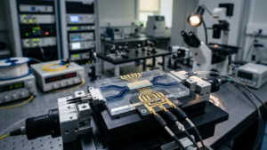
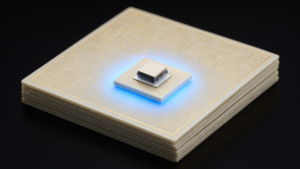
A research team led by Professor Miro Erkintalo of the University of Auckland, in collaboration with the University of Maryland and the US National Institute of Science and Technology, has demonstrated a viable path for miniaturizing optical frequency combs to a chip-scale architecture. The team successfully used the chip-based system to perform three core tasks: generating precise optical frequencies, producing low-noise millimetre-wave signals, and integrated optical clock readout.
Technical Details
The new design departs from conventional architectures where light from a single laser cascades outward to cover a spectrum. Instead, this approach utilizes two lasers positioned an octave apart (a doubling of frequency) at opposite ends of the spectrum. The system automatically fills in the light frequencies between these two boundaries, overcoming the control and stabilization challenges that have previously hampered chip-integrated combs. This proof-of-concept, which began as a prediction in 2021 and was demonstrated in the lab in 2024, was further refined in 2026 to realize these breakthrough applications.
Background & Context
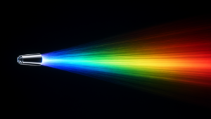
Optical frequency combs, pioneered in the late 1990s by Nobel Prize winners John Hall and Theodor Hänsch, act as “light rulers” by creating millions of perfectly spaced frequencies of light. While these tools are essential for measuring time, distance, and chemical signals with extreme accuracy, their size and expense have historically confined them to laboratory environments.
Significance & Outlook
Reducing the size, weight, power, and cost of this technology enables mass production and consumer-level deployment. Potential applications include:
- Portable optical atomic clocks for mapping underground mineral deposits.
- Navigation systems that operate independently of GPS satellite signals.
- Synchronization in telecommunications networks.
- Precision sensors capable of detecting minute environmental changes.
Erkintalo, Moille, and Srinivasan have submitted a provisional patent application based on this work.
Source: https://www.photonicsonline.com/doc/university-s-research-advances-ultra-precision-laser-tech-0001
Get our weekly technology intelligence — free
Receive an infographic that lets you judge at a glance whether each field’s analysis report is worth reading.
Subscribe Free — Weekly Tech Intelligence
By subscribing, you’ll receive Troy-Technical’s weekly technology intelligence newsletter.
- Your email and selected fields are used only to deliver the newsletter.
- We never share your information with third parties.
- You can unsubscribe anytime via the link in each email.
See our Privacy Policy for details.
Takes about a minute · Unsubscribe anytime