Key Findings
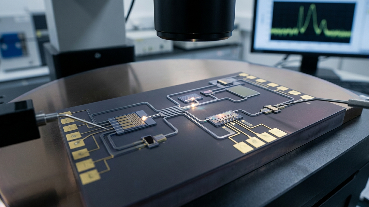
III-V quantum dot (QD) photodetectors have garnered significant attention for on-chip sensing in the telecom O-band due to their high responsivity and low dark current characteristics. Researchers have now successfully demonstrated the first monolithic integration of III-V QD photodetectors and QD lasers on silicon nitride waveguides. This integration fundamentally simplifies the design and manufacturing of photonic integrated circuits (PICs).
Technical and Business Details
- Achieving Monolithic Integration: The core of this research lies in fabricating both the QD laser and QD photodetector from the same III-V layer stack. This approach bypasses the complexities of hybrid integration, where separate devices are later coupled, allowing for the formation of a single device with both functionalities through a unified manufacturing process. This monolithic integration substantially contributes to device miniaturization, enhanced reliability, and reduced manufacturing costs.
- High Responsivity and Low Dark Current: The developed QD photodetector exhibits both high responsivity (high sensitivity to optical signals) and low dark current (minimal leakage current in the absence of light). These characteristics are crucial for enabling more sensitive and precise detection in optical communication systems and sensor applications.
- Telecom O-Band Compatibility: The telecom O-band (approximately 1260-1360 nm) is one of the primary wavelength windows for optical fiber communication. Enabling on-chip sensing in this band allows for the integration of real-time monitoring and diagnostic functionalities within optical communication systems, thereby improving network operational efficiency and reliability.
- Replacing Germanium Photodetectors: Traditionally, germanium (Ge)-based photodetectors were commonly used for O-band optical detection in silicon photonics platforms. However, the integration of Ge detectors into Si photonics processes presented challenges. The new III-V QD detector approach eliminates this need, offering a more efficient integration pathway.
Background and Industry Context
Photonic Integrated Circuits (PICs) are increasingly vital across various fields, including data communication, sensing, and quantum technologies. However, efficiently and densely integrating light sources (lasers) and light detectors (photodetectors) has been a long-standing challenge. Particularly, directly forming high-performance light sources and detectors on silicon substrates has proven difficult, leading to a prevalence of hybrid integration. This monolithic integration offers a groundbreaking solution to this challenge.
Strategic Significance and Outlook
This monolithic integration technology for III-V QD photodetectors and lasers is expected to significantly impact the design of next-generation optical communication modules, on-chip sensors, and even quantum information processing devices. The simplification of the manufacturing process and enhancement of device performance are poised to accelerate the commercialization of these technologies, enabling smaller, higher-performance, and lower-cost optoelectronic systems. This represents a broad innovation driver within the photonics field.
Get our weekly technology intelligence — free
Receive an infographic that lets you judge at a glance whether each field’s analysis report is worth reading.
Subscribe Free — Weekly Tech Intelligence
By subscribing, you’ll receive Troy-Technical’s weekly technology intelligence newsletter.
- Your email and selected fields are used only to deliver the newsletter.
- We never share your information with third parties.
- You can unsubscribe anytime via the link in each email.
See our Privacy Policy for details.
Takes about a minute · Unsubscribe anytime








Comments