Key Findings
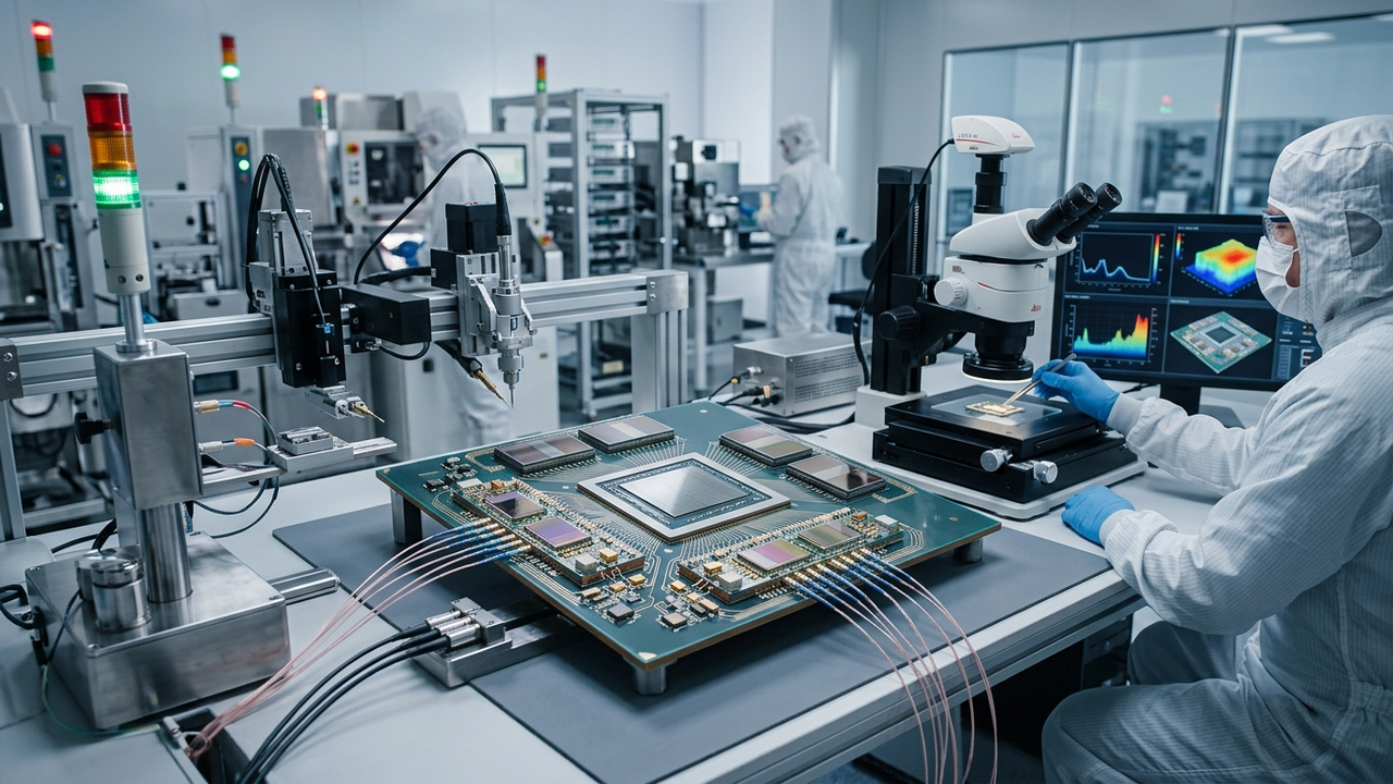
TSMC is aggressively accelerating the deployment of Co-Packaged Optics (CPO) as GPU and ASIC computing power confronts the physical limitations of conventional copper interconnects. The company is integrating CPO with its suite of advanced packaging technologies, including 3DFabric, CoWoS, SoIC, and silicon photonics, to advance system-level integration solutions that seamlessly connect computing units, HBM memory, and high-speed I/O.
Technical / Clinical Details
CPO dramatically reduces power consumption and significantly boosts bandwidth by substantially shortening electrical interconnect paths and transmitting data via optical fibers. TSMC’s strategy involves combining CPO with cutting-edge silicon wafer-level packaging (3DFabric), chiplet integration (CoWoS and SoIC), and silicon photonics—which integrates optical and electronic circuits. This approach enables AI/HPC chips to process enormous data volumes with lower power and reduced latency. However, mass production of CPO necessitates overcoming key technical challenges, including high-precision packaging of optical components, stable optical coupling with the chip, and establishing efficient testing methodologies at manufacturing scale.
Background & Context
The surging demand for AI and High-Performance Computing (HPC) has driven GPUs and ASICs to unprecedented levels of performance. Yet, the data transfer speed between chips has emerged as a critical bottleneck, hindering overall system performance gains. Traditional electrical interconnects are approaching their limits in terms of signal degradation and power consumption, making optical interconnects the anticipated next-generation standard for resolution. TSMC’s focus on CPO is a strategic move by a leading semiconductor manufacturer to spearhead the evolution of computing performance in the AI era, poised to have a profound impact on the entire industry.
Strategic Significance & Outlook
TSMC’s aggressive investment and integration of CPO technology hint at the potential for a ‘CPO Moore’s Law,’ where advancements in optical interconnect technology could create a new growth curve for computing performance. If challenges in packaging, optical coupling, and testing are successfully addressed, CPO is set to become a standard interconnect solution in data centers, AI supercomputers, and other high-performance computing applications. This will contribute to the further evolution of AI and the realization of previously impossible computational capabilities, forming a foundational pillar for next-generation digital infrastructure.
Source: https://www.kucoin.com/news/flash/tsmc-accelerates-cpo-layout-industry-eyes-new-cpo-moore-s-law
Get our weekly technology intelligence — free
Receive an infographic that lets you judge at a glance whether each field’s analysis report is worth reading.
Subscribe Free — Weekly Tech Intelligence
By subscribing, you’ll receive Troy-Technical’s weekly technology intelligence newsletter.
- Your email and selected fields are used only to deliver the newsletter.
- We never share your information with third parties.
- You can unsubscribe anytime via the link in each email.
See our Privacy Policy for details.
Takes about a minute · Unsubscribe anytime





Comments