GPU– tag –
-

Samsung Electro-Mechanics and Qualcomm Jointly Develop Organic Bridge for Advanced 2.1D AI Semiconductor Packaging
The Elec South Korea Overview Samsung Electro-Mechanics and Qualcomm have collaborated to develop an 'organic bridge' technology for advanced 2.1D packaging in AI semiconductors. This innovation facilitates high-density, high-bandwidth i... -
AI Infrastructure Component Crunch Becomes Reality: ABF Substrate Lead Times Hit 56 Weeks, Equipment Parts Up to 40 Months
BigGo Finance Taiwan Overview The supply shortage for AI infrastructure components is becoming entrenched; TrendForce reports ABF substrate lead times surged to 48–56 weeks, approximately 4 to 4.7 times the equilibrium. HDDs reached 50 w... -
Samsung Electro-Mechanics Unveils Next-Gen Package Substrate Technologies for AI & Servers at KPCA Show 2026, Highlighting Warp Reduction & High-Density Interconnects
Samsung Electro-Mechanics South Korea Overview Samsung Electro-Mechanics showcased a comprehensive suite of next-generation semiconductor package substrate technologies targeting the AI and server markets at 'KPCA Show 2026.' The company... -
Nvidia Chip Sales Projected to Double Next Year, Accelerating HBM4 Transition Amid TSMC CoWoS Packaging Bottleneck
No source name USA Overview Nvidia CEO Jensen Huang forecasts a doubling of Nvidia chip sales next year and an accelerated transition to HBM4, with TSMC's CoWoS advanced packaging identified as a primary shipping bottleneck. CoWoS is cru... -
HBM Identified as Primary Bottleneck for AI Chip Manufacturing; Nvidia, Google, AMD, Amazon Consumed 90% of Global Supply in 2025
New Market Pitch USA Overview High Bandwidth Memory (HBM) has emerged as the most significant bottleneck in AI chip manufacturing, surpassing advanced packaging technologies like CoWoS. According to Epoch AI estimates, just four companie... -
TSMC Accelerates Co-Packaged Optics (CPO) Deployment, Eyes ‘CPO Moore’s Law’ for AI Chip Performance Boost
KuCoin Taiwan Overview As GPU and ASIC computing power continues to advance, TSMC is accelerating the deployment of Co-Packaged Optics (CPO) to address the power consumption and signal transmission limits of traditional copper interconne... -
Intel and Ayar Labs Propel 224Gbps+ Scale-Up with Co-Packaged Optics, Extending NVIDIA NVLink
Silicon Co-Design USA Overview Co-Packaged Optics (CPO) technology is enabling 224Gbps+ scale-up interconnects, with Intel pursuing a truly integrated approach via its Optical Compute Interconnect (OCI) that heterogeneously integrates In... -
NTT West Expands “All-Photonics Connect powered by IOWN” Service Across Western Japan to Bolster AIOWN Infrastructure
ASCII Japan Overview NTT West is set to expand its "All-Photonics Connect powered by IOWN" Type 3 and Type 4 services across the entire western Japan region, beginning with Hokuriku in September 2027 and Shikoku in January 2028. This exp... -
NVIDIA Adopts Hybrid Copper-Optics Strategy for AI Factories, NVLink 6 Connects 72 GPUs with Multi-Layer Resiliency
Elliot's Musings USA Overview NVIDIA is implementing a hybrid interconnect strategy for its AI factories, utilizing both extensive copper cabling for NVLink to connect 72 GPUs and developing integrated optical engines closer to switching... -
FS Unveils 1.6T Scale-Out Optics with 500 km Coherent Modules for AI Fabrics, Validated on NVIDIA Quantum-X800
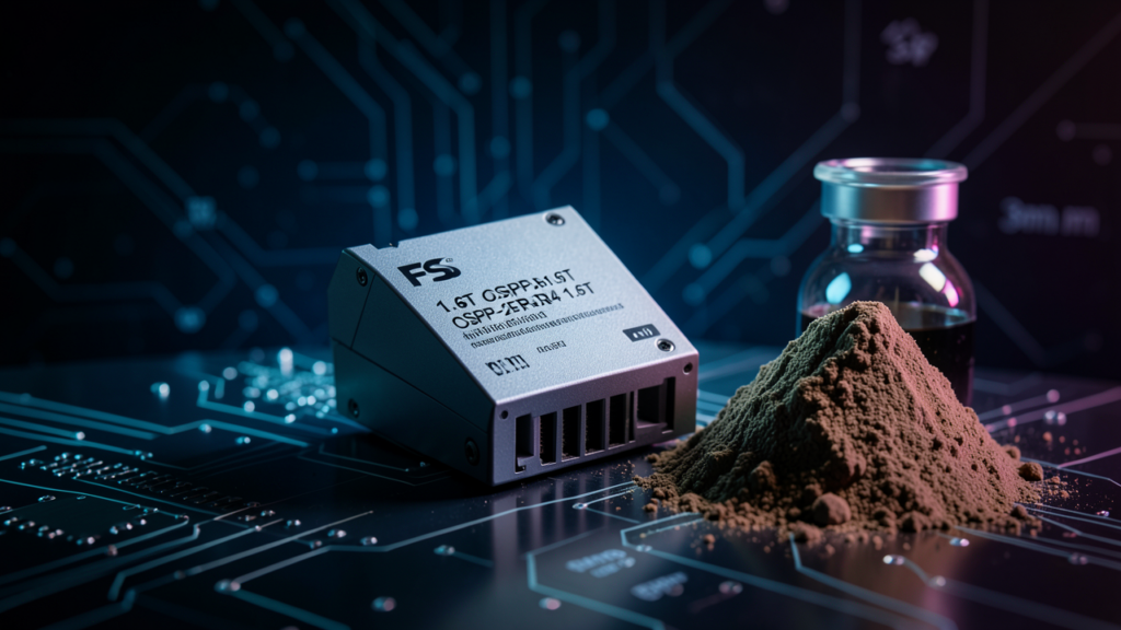
StorageReview.com USA Overview FS has introduced a new AI optics portfolio featuring 1.6T scale-out transceivers for GPU cluster links and 500 km coherent modules for inter-site connections. The 1.6T OSFP-DR8-1.6T and OSFP-2FR4-1.6T modu...