SEMICONDUCTOR FABRICATION · INTRODUCTION 1-2
Semiconductor Types and Applications
Why a processor, an electric car and an LED need different materials - and how the job determines the device and the way it is made.
- Start with the job, then choose the material
- Seven roles to keep in mind
- Logic: making many small decisions
- Memory: keep charge, and read it reliably
- Analogue: listen carefully to the real world
- Power electronics: control energy on its way to useful work
- Why SiC is useful in EV and motor drives
- The same idea beyond the car
- GaN: a different route to fast power conversion
- Sensors: turn a physical change into an electrical signal
- Optoelectronics: choose the layer that produces the light
- RF: amplify the signal without losing the information
- A material guide you can reason from
- Different jobs require different fabrication priorities
- Check your understanding
- A short glossary
- Sources and scope
Begin with the main text. The shaded physics boxes add optional detail and worked estimates. Figures are conceptual and not to scale. Numbered links lead to the supporting sources.
Recognise seven useful semiconductor roles; connect each role to a material property and a device structure; explain what an EV inverter does and why SiC can help; and see why different products place different demands on fabrication. Introduction 01 provides the background on bands, carriers, junctions and transistors.
Start with the job, then choose the material
A mobile phone, an electric car and a broadband connection all depend on semiconductors. Yet the same material is not equally good at every task. A processor must make billions of small switches work together. A motor drive must repeatedly block a high voltage and carry a large current. A laser must turn electrical energy into light at a useful wavelength.
The question to ask is therefore “What must this device do?” Follow that with “What makes the job difficult?” Only then does the material choice begin to make sense.
| Everyday situation | The job | A useful material property |
|---|---|---|
| Editing a photograph on a phone | Perform many logical operations efficiently | Silicon supports controllable interfaces and dense, repeatable circuits |
| Accelerating an electric car | Deliver controlled power from battery to motor | SiC supports high-voltage blocking with a relatively low-resistance power-device structure |
| Using a compact laptop charger | Convert power efficiently in a small enclosure | GaN devices can combine voltage capability with low switching charge |
| Sending a mobile signal | Amplify a rapidly varying radio signal | GaAs and GaN offer useful transport and device properties for different RF requirements |
| Lighting a room or sending data through fibre | Produce light at a chosen wavelength | Compound-semiconductor active layers can be engineered for efficient emission |
The material is only one part of the answer. A suitable structure, good interfaces, reliable contacts, packaging and a practical manufacturing process must turn that potential into a useful product.
Logic, memory and power describe jobs. Silicon, SiC and GaN describe materials. One material can do several jobs, and one job can be done using several materials. Do not put “logic” and “SiC” on the same list as though they were competing categories.
Seven roles to keep in mind
For learning purposes, we will use seven broad roles. They overlap: a camera contains sensors, analogue circuits, logic and memory; a power-management chip can combine control circuitry with power devices.
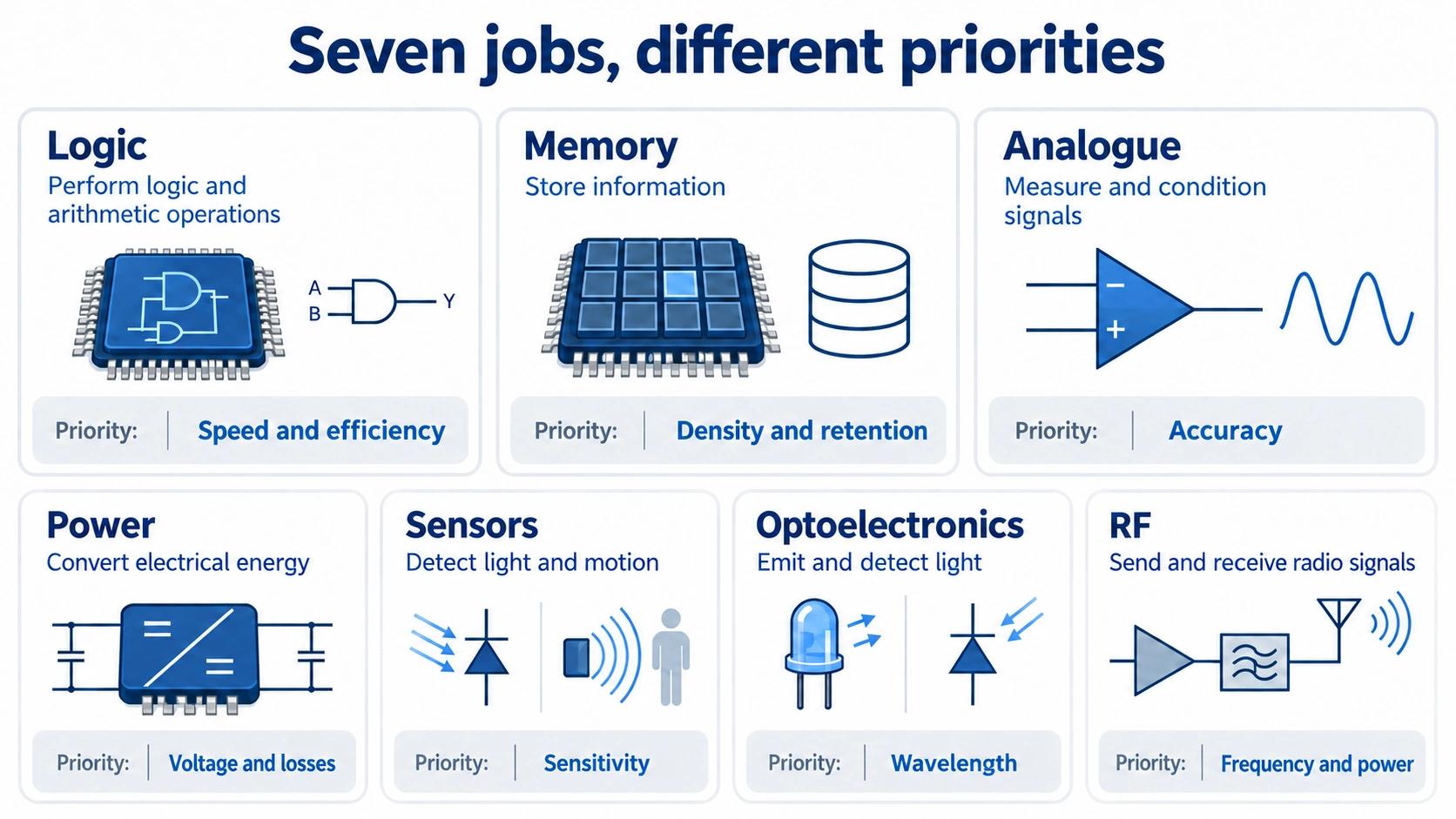
Industry statistics use their own categories. WSTS, for example, separates microprocessors and microcontrollers into a “micro” category rather than putting every computing chip under “logic”. It also groups products differently from our seven-role teaching map. [1]
This chapter concentrates on the physical reasons for device choices. Market forecasts and product-generation announcements change quickly; they are less useful than the underlying principles for learning why a material belongs in a particular application.
Logic: making many small decisions
A logic circuit represents information using electrical states and combines those states to perform operations. CPUs run instructions; GPUs apply many operations in parallel; an SoC, or system-on-chip, integrates several functions within one chip. A microcontroller adds processing, memory and peripherals for embedded control.
The central challenge is not simply to make one exceptionally fast transistor. It is to make a very large number of transistors switch predictably, connect them, and keep the total power manageable.
Why silicon remains the foundation
Silicon's great advantage is the combination of useful electronic behaviour with a highly developed system of insulating films, interfaces and fabrication methods. A gate must control a channel without becoming an unwanted conducting path into it. Silicon dioxide helped make that control practical and reproducible. Advanced devices also use high-k dielectrics and metal gates; a “silicon chip” is a carefully arranged combination of materials. [2]
Large, high-quality silicon wafers and a mature manufacturing infrastructure allow enormous numbers of devices to be fabricated consistently. Silicon's success cannot be explained by electron mobility alone. Another material may transport electrons more readily yet be harder to integrate into dense, low-leakage, complementary logic.
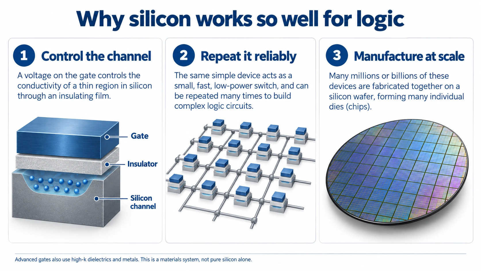
A useful estimate for dynamic CMOS power is P ≈ αCV²f, where α describes switching activity, C is the capacitance being switched, V is supply voltage and f is frequency. Keep the other terms fixed and reduce V from 1.0 V to 0.8 V: the dynamic term becomes 0.8² = 0.64, a reduction of 36%. [3]
Lower voltage also makes it harder to switch quickly and maintain comfortable noise margins. Leakage and interconnect losses remain. Smaller features can help, but shrinking a transistor does not automatically reduce every part of the chip's power budget.
Leading logic processes put great effort into gate control, fine patterning and dense interconnect. FinFET and gate-all-around structures help the gate control a short channel. Process names such as “3 nm” are generation labels, not the dimensions of every feature on a chip.
Memory: keep charge, and read it reliably
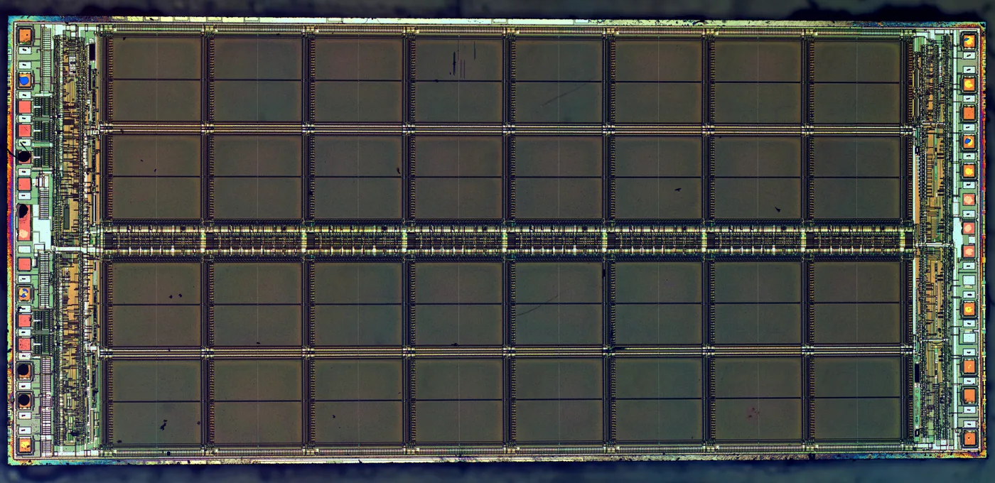
A computer needs both a working area and persistent storage. DRAM provides rapidly accessible working memory but loses its contents without power. NAND flash keeps information after power is removed and is used in SSDs, phones and other storage products. These are different compromises, not simply fast and slow versions of the same cell.
DRAM: a small electrical store that needs attention
A conventional DRAM cell uses an access transistor and a capacitor. A stored amount of charge changes the signal sensed when the cell is read. Logical states are distinguished electrically; “1” does not mean exactly one electron, and “0” does not mean an absolutely electron-free cell.
Charge leaks away. The memory must periodically restore its contents through refresh. Making the cell smaller makes the storage and sensing problem more difficult. Designers use three-dimensional capacitor structures and suitable dielectric materials to retain enough capacitance within a small footprint. [4]
NAND: stored charge changes a transistor's behaviour
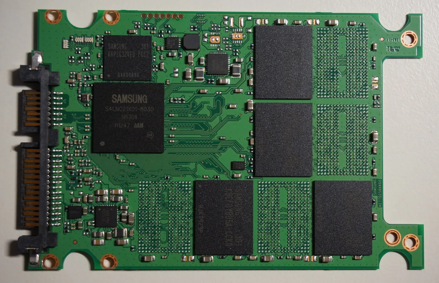
NAND flash stores charge in an isolated storage region. In a charge-trap structure, electrons are held in trapping sites within a material layer. Their presence changes the transistor's threshold voltage. Reading the cell means distinguishing threshold-voltage ranges.
Programming and erasing use strong electrical fields to move charge across an insulating barrier through quantum processes such as tunnelling. A strong field changes the barrier seen by the electrons; it does not mechanically open a hole in the film. During retention, the barrier makes escape sufficiently unlikely for useful storage, although charge loss and defects remain important over time. Repeated programming and erasing can damage the dielectric, so endurance is finite.
More bits per cell require more distinguishable states. TLC stores three bits, requiring 2³ = 8 threshold ranges. QLC stores four bits, requiring 16. The more ranges we fit into the available window, the tighter the requirements on sensing, interference, error correction and charge retention.
Two quite different meanings of stacking
In 3D NAND, memory cells are formed through a multilayer structure within a die. A vertical channel passes through many word-line levels; the surrounding films provide charge storage and insulation. Fabrication must form deep, narrow features and deposit uniform films through complex structures. Some processes build and connect several stack sections rather than etching every layer in one operation. [5]
In HBM, or high-bandwidth memory, separate DRAM dies are stacked and connected with many vertical interconnects. The stack sits close to a processor and provides a very wide data path. It helps address the problem of supplying data fast enough for intensive computation. It is still DRAM and still requires power and refresh.
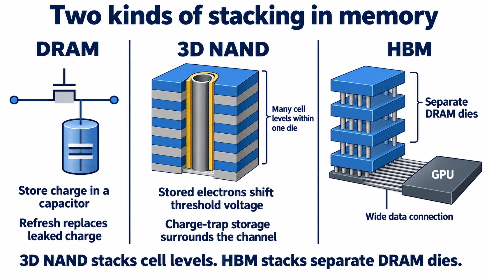
Both products involve silicon, but the critical work differs. DRAM must store and sense small charges. NAND must hold and repeatedly alter threshold states. HBM must also move data through dense connections and manage heat in a package. “Made from silicon” is far too broad to describe how any of them is manufactured.
Why does AI computing rely on GPUs rather than CPUs? Why has HBM become essential? And what happens when data movement, heat and power can no longer keep up with arithmetic speed? These questions are the subject of the next lesson, Introduction 1-3, “Semiconductors in the AI Era”.
Analogue: listen carefully to the real world
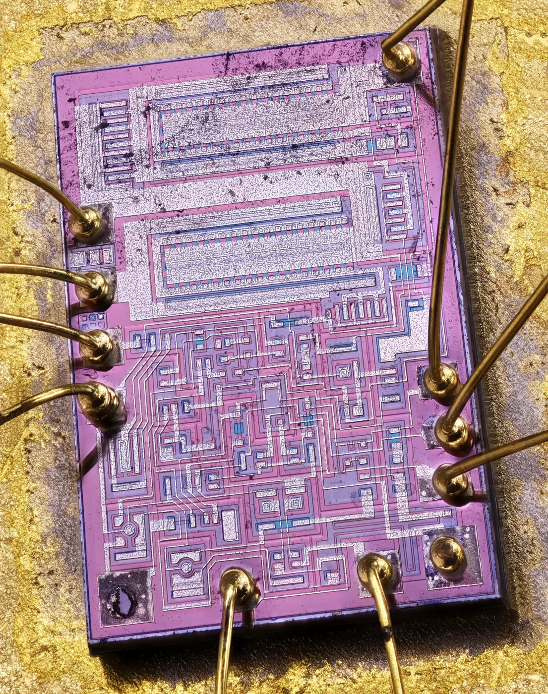
Sound, light intensity, temperature and battery voltage vary continuously. Analogue circuits amplify, filter, compare or regulate electrical signals representing those quantities. Analogue-to-digital converters then turn measured values into digital numbers.
Think of a microphone signal. A circuit that amplifies it must preserve the useful variation without adding too much noise or distortion. Its behaviour should remain predictable as temperature and supply voltage change. A power-management circuit may also need to handle voltages far above those used by a processor core.
Why the smallest transistor is not always the best answer
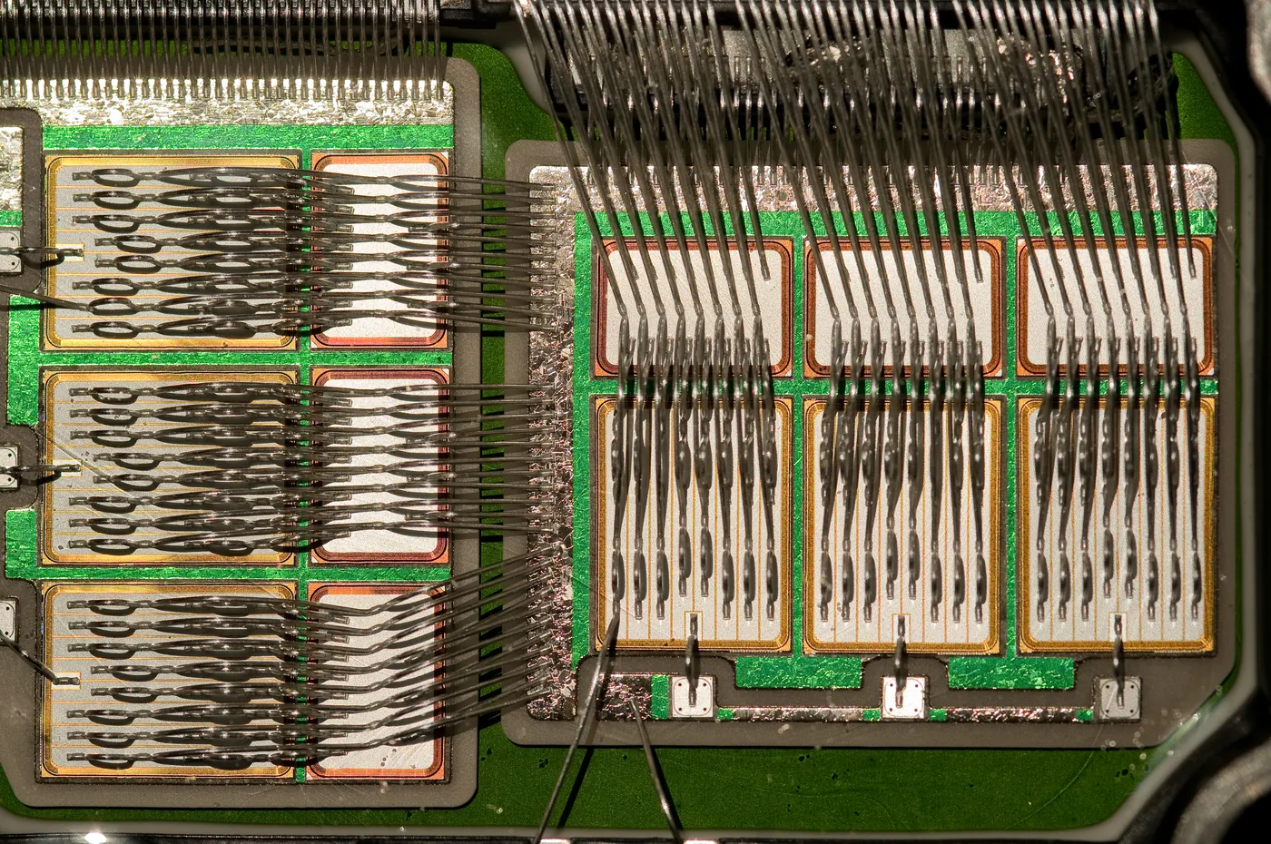
Analogue design often values matching, low noise, voltage headroom and stable passive components more than maximum transistor density. Larger devices can help reduce some sources of mismatch and noise. Specialised silicon processes can combine precision circuitry with higher-voltage devices.
This is why many analogue products use well-established process generations. That does not make them technologically trivial. Precision, reliability, characterisation and cost are demanding engineering problems. Some high-speed converters and RF circuits use advanced processes; there is no rule that all analogue belongs on an older node.
Silicon is useful here because many complementary devices, resistors and capacitors can be integrated within a controlled process. The material choice serves the complete circuit, not an isolated mobility figure.
Power electronics: control energy on its way to useful work
A power semiconductor switches or rectifies electrical energy in a converter. Applications include motor drives, renewable-energy systems, vehicle chargers, server power supplies and domestic appliances. The voltage and current requirements vary enormously across these uses.
Common choices include power MOSFETs and insulated-gate bipolar transistors, or IGBTs. A MOSFET is controlled through an insulated gate; an IGBT combines gate control with bipolar conduction. Their trade-offs depend on voltage, current and switching conditions.
A processor's logic switch communicates a state. A traction inverter's power switch must handle substantial energy flowing towards a motor. Both use field control, but they are engineered for very different operating conditions.
First understand the EV, then the inverter
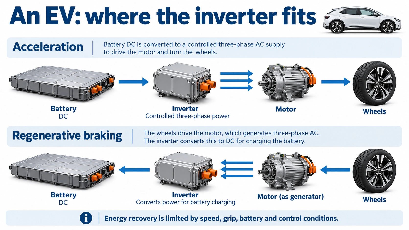
An EV battery provides direct current, or DC: its terminals have a defined polarity. Many traction motors use three sets of windings, or phases, supplied with carefully timed currents. Together those currents create a rotating magnetic field that produces torque.
The traction inverter sits between the battery and the motor. It uses controlled power switches to apply voltages to the motor phases and regulate their currents. Calling it a “DC-to-AC converter” is correct, but only the beginning: it must deliver the right current at the right time for the motor's operating conditions. During regenerative braking, the power flow can reverse. [6]
What changes when you press the accelerator?
The accelerator pedal sends a request to the control system. Sensors and control software determine how to operate the inverter using information such as rotor position and phase current. The pedal is not a mechanical valve that simply opens a wider path from battery to motor.
A common three-phase inverter uses three pairs of upper and lower switching positions. Each position may contain several semiconductor dies. By switching these positions in a coordinated pattern, the inverter produces voltage pulses at the motor terminals.
The motor windings have inductance, which resists rapid changes in current. The controller adjusts the pulses so that the resulting currents produce the required torque. One common method is pulse-width modulation, or PWM: changing the time spent in selected switching states changes the effective voltage applied over a short interval.
The semiconductor switching frequency, the electrical frequency associated with the rotating field, and the rotor's mechanical speed are different quantities. Motor pole count and motor type connect the latter two; the controller coordinates them. Doubling the switching frequency does not simply double the speed of the car.
During braking, the wheels can drive the motor as a generator. The inverter controls the return of electrical energy to the DC side. Regeneration recovers part of energy the vehicle already had; it does not create energy. Battery state of charge, temperature, available grip and control limits constrain recovery. Friction brakes are still required. [6]
SiC belongs in the inverter's power switches. It is not the name of the motor's magnets or the battery chemistry. Once its location is clear, the reason for choosing it becomes easier to understand.
Why SiC is useful in EV and motor drives
Silicon carbide, SiC, is a compound semiconductor made from silicon and carbon. The 4H-SiC crystal form is widely used for power devices. Its band gap is roughly 3.2-3.3 eV, compared with about 1.12 eV for silicon, and it has a much higher critical electric field. Those properties help a properly designed device block high voltage while keeping its conducting resistance manageable. [7]
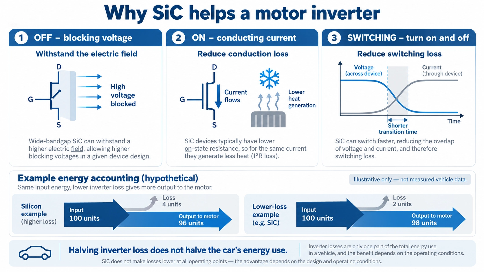
The inverter's switches repeatedly face three different jobs.
| Operating state | The difficulty | What a SiC MOSFET can offer |
|---|---|---|
| Off | Sustain a large voltage without unwanted breakdown | A high critical field permits a thinner, more highly doped blocking region |
| On | Carry current without wasting too much energy as heat | Lower resistance can reduce conduction loss at a chosen voltage rating |
| Changing state | Voltage and current can overlap during transition | A suitable device and gate drive can reduce switching energy compared with an appropriate silicon reference |
When the switch is on: resistance costs energy
For a MOSFET, a first estimate of conduction loss is P ≈ I²R, using the relevant on-resistance and current waveform. A large current makes resistance especially important. Double the current at unchanged resistance and the instantaneous resistive loss becomes four times larger.
For example, 100 A through 5 mΩ gives 50 W; through 2.5 mΩ it gives 25 W. These are deliberately simple component calculations, not a whole-inverter model or specifications for particular devices. In a real drive, current varies, conduction is shared among devices, and resistance changes with temperature.
When it changes state: resistance is not the whole story
A switching device takes finite time to change between blocking voltage and carrying current. The integral of voltage multiplied by current over the transition gives an important part of the switching energy. Capacitances must also be charged and discharged, and commutation behaviour matters.
Silicon IGBTs use minority-carrier injection to reduce conducting resistance at high voltage. Stored charge can then contribute to turn-off losses. A SiC MOSFET normally uses majority-carrier conduction, avoiding that particular IGBT trade-off, although capacitance, diode behaviour, parasitic inductance and drive losses remain. The comparison depends on device ratings and operating conditions. [8][9]
As a simple illustration, 1 mJ per switching cycle × 10,000 cycles per second = 10 W. The same assumed energy at 20,000 cycles per second gives 20 W. Real switching energy itself varies with voltage, current, temperature and gate drive. This explains why “switch faster” is a design decision with consequences, not an unconditional benefit.
When it is off: why a stronger field helps
In a strong field, carriers can gain enough energy between scattering events to generate additional electron-hole pairs through impact ionisation. A multiplying avalanche current can follow. The relevant critical field depends on the material and device conditions. A wider gap is associated with useful high-field capability, although a band-gap value alone does not specify the breakdown voltage of a finished transistor.
Voltage is the accumulated change in electrical potential through a region. A higher allowable electric field lets a device sustain a given voltage over a shorter distance. In a power device, a lightly doped drift region often provides much of that blocking capability.
Representative teaching values are about 0.3 MV/cm for silicon's critical field and 3 MV/cm for 4H-SiC. For a simplified triangular field distribution, V ≈ ½EcritW, so W ≈ 2V/Ecrit. [7]
At 1000 V, this gives about 67 µm for silicon and 6.7 µm for SiC. These are idealised drift-region estimates. They are not total chip thicknesses, guaranteed product dimensions or a substitute for a real breakdown design with edge termination and safety margins.
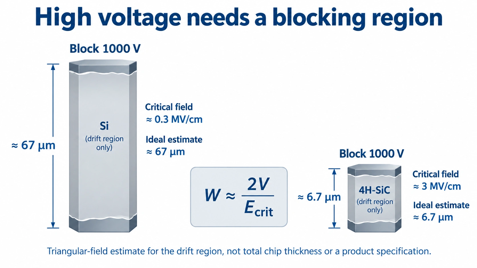
A thinner path reduces resistance. The high critical field also allows a higher drift-region doping concentration for a given blocking requirement, making that path easier to conduct through. This is a key physical route to lower specific on-resistance. Actual resistance also includes channel, contact and other contributions. A material figure of merit is not a prediction of the efficiency of a complete car.
Wide band gap is a useful clue to high-field capability, not a stand-alone explanation of all performance. Thermal conductivity, interfaces, crystal defects, device geometry, packaging and reliability all matter. Even a material capable of tolerating high temperatures is limited by the complete module's permitted operating conditions.
A real vehicle example, with the comparison kept in context
In March 2023, DENSO announced an inverter using SiC power semiconductors for the Lexus RZ through BluE Nexus's eAxle drive module. The company reported inverter power losses less than half those of its conventional silicon-based comparison under specified driving conditions. This was a claim about that converter comparison, not a halving of the car's total energy use or a guarantee for every later model. [10]
Imagine a converter receiving 100 units of energy and losing four, leaving 96 for its output. Cut that loss to two and the output becomes 98. The loss has halved; the useful output has increased from 96 to 98. This hypothetical example explains the language of efficiency claims. It is not a measurement of the Lexus vehicle.
Less loss can improve usable energy and ease cooling requirements. Designers might use that margin for longer range, a smaller cooling system or higher sustained output. The vehicle-level result depends on the entire drive system, driving cycle, mass and thermal design.
The same idea beyond the car
Motor drives also appear in heat pumps, air conditioning, factory machinery, pumps, fans and trains. They vary electrical supply conditions to control how much mechanical work a motor performs. [11]
| Equipment | What variable-speed control achieves | Where semiconductor choice enters |
|---|---|---|
| Heat pump or air conditioner | Adjusts compressor operation to heating or cooling demand | Converter loss, cost, noise and thermal design influence the device choice |
| Pump or ventilation fan | Matches flow to actual demand | Running the motor appropriately saves energy; the converter's own losses are a separate issue |
| Factory conveyor | Controls movement, torque and speed | Duty cycle, reliability and total system cost matter |
| Electric train | Controls traction and can return braking energy | High-voltage SiC modules are one practical option for traction systems [12] |
There are two different energy-saving mechanisms here. First, operating a motor only as hard as the process needs can reduce the mechanical energy demand. Second, reducing losses inside the converter wastes less of the energy used to meet that demand. SiC primarily addresses the second mechanism; it does not by itself decide the best pump speed.
Not every drive needs SiC. Silicon MOSFETs and IGBTs remain useful where their performance, cost and reliability fit the job. Fast edges can also make electromagnetic interference and motor-insulation stress harder to manage. The complete drive must be designed around the device.
GaN: a different route to fast power conversion
Gallium nitride, GaN, is another wide-band-gap material. Many power GaN transistors use a HEMT structure with a thin electron channel near a semiconductor interface, rather than simply copying a vertical silicon or SiC MOSFET.
Suitable GaN devices can combine high-field capability with small switching charge and low parasitic capacitances. That can support efficient high-frequency conversion. Higher switching frequency can allow smaller magnetic components, helping explain compact chargers. It does not remove magnetic, thermal or filtering requirements, and it does not guarantee that every GaN supply is smaller or more efficient. [13]
For comparison, vertical SiC MOSFETs are well suited to many high-voltage, high-current applications, including traction. Lateral GaN HEMTs provide another valuable combination of structure and properties. Voltage, current, switching frequency, packaging and cost determine the practical choice; the material names are not a universal ranking.
We will return to the HEMT channel in the RF section, because a related material system can also amplify radio signals. A power-switching device and an RF amplifier have different design priorities even when both use GaN.
Sensors: turn a physical change into an electrical signal
A sensor needs to respond predictably to something outside the circuit. Light, acceleration, pressure and rotation can all be converted into electrical signals, but they do not all use the same physical mechanism.
Image sensors: collect light-generated charge
A silicon photodiode can absorb visible light and generate electron–hole pairs. A camera pixel collects charge and uses readout circuitry to turn it into an electrical measurement. Silicon is particularly useful because the photosensitive regions can be combined with sophisticated CMOS circuitry. The useful result depends on absorption, collection, noise and readout, not just on the band-gap value. [14]
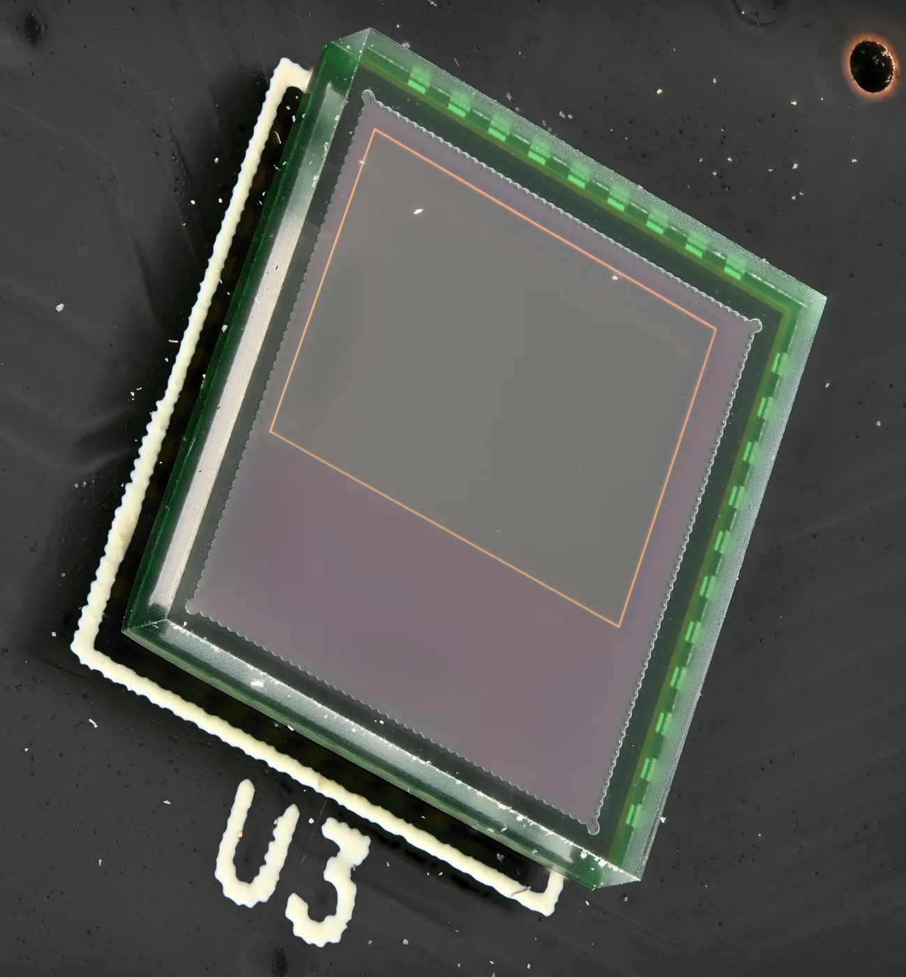
In a front-illuminated arrangement, light approaches through the side containing interconnect, which can obstruct or complicate the optical path. In a back-illuminated arrangement, the wafer is thinned and light enters from the opposite side, reaching the photosensitive silicon before the wiring. [14]
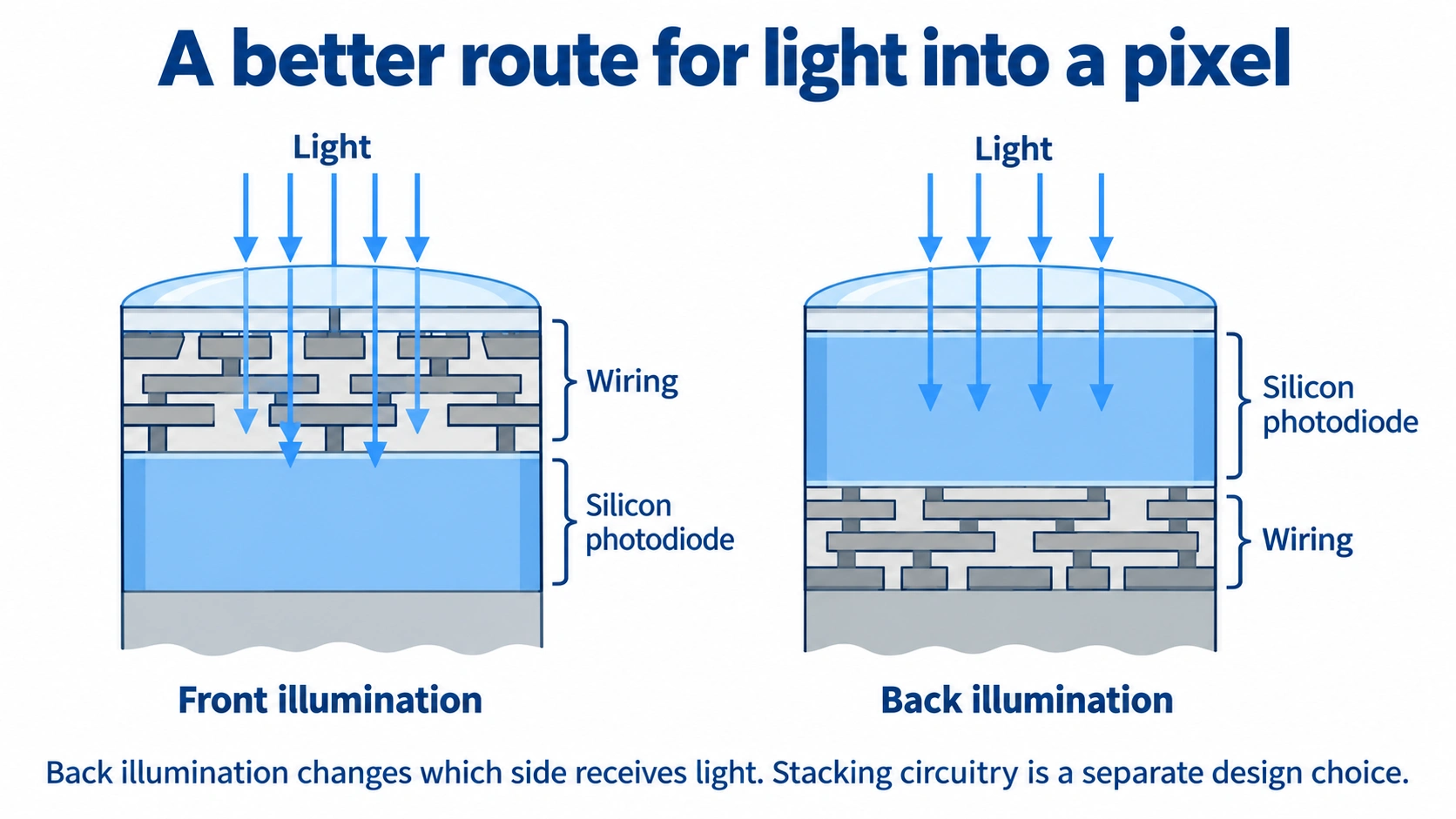
A stacked image sensor can put the pixel array and processing circuitry on separate bonded layers, allowing each to be optimised. Wafer thinning, low-defect surfaces, bonding accuracy and electrical connections then become essential fabrication requirements.
MEMS: silicon can also act as a spring
MEMS means microelectromechanical systems. Fabrication methods create tiny moving masses, beams, membranes or comb-shaped electrodes. Silicon is useful not only because it is a semiconductor, but also because small crystalline structures can provide predictable mechanical behaviour.
In a capacitive accelerometer, acceleration displaces a suspended mass. That changes the geometry of electrodes and therefore their capacitance. A readout circuit measures the change. This is mechanical motion converted into an electrical measurement, not light exciting electrons across a band gap.
A vibrating MEMS gyroscope senses rotation through Coriolis-related motion: rotation couples a driven movement into a detectable motion in another direction. Precise structures and signal processing extract the rotation rate. [15]
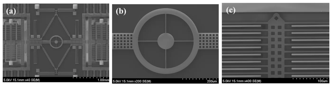
Deep etching, releasing moving parts, controlling stress and protecting the mechanism in a package matter as much as making transistors. MEMS is a useful reminder that semiconductor processing can create functional geometry, not just electronic junctions.
Optoelectronics: choose the layer that produces the light
LEDs and semiconductor lasers convert electrical energy into light. In an efficient emitter, the active region provides a favourable radiative recombination path for electrons and holes. A suitable direct-band-gap material helps. Silicon's indirect band gap makes conventional efficient light emission difficult, even though silicon works well in many light detectors.
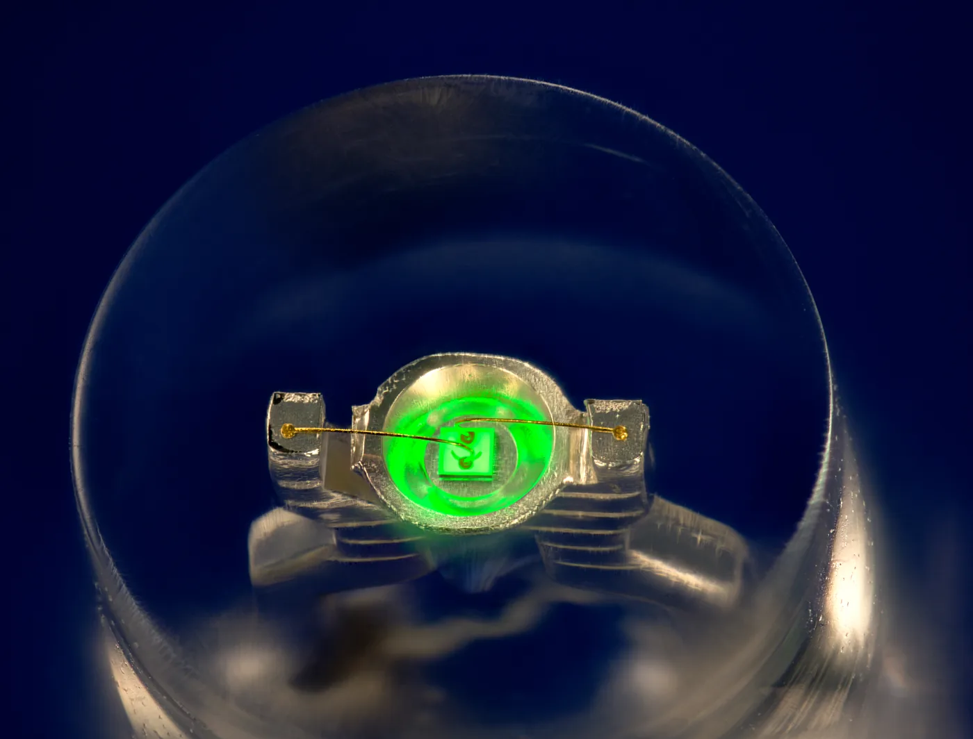
Why blue LEDs and fibre-optic lasers use different layers
Photon energy and wavelength are related by E(eV) ≈ 1240/λ(nm). Blue light around 450 nm corresponds to about 2.76 eV. Telecom light at 1550 nm corresponds to about 0.80 eV. Those are quite different energy targets.
An InGaN active region can be engineered for blue or green emission within a GaN-based structure. Composition and quantum-well design influence the transition energy. Pure bulk GaN's band gap should not be used as though it were the emission energy of every blue LED. The 2014 Nobel Prize in Physics recognised the invention of efficient blue LEDs, which enabled bright, energy-saving white light sources. [16]
For fibre-optic communication, InP-based material systems allow suitable layers for near-infrared emission and detection. For example, an InGaAsP active region can provide laser emission near 1.55 µm on an InP substrate. InGaAs can serve as the absorbing region of a detector on InP. [17][18]
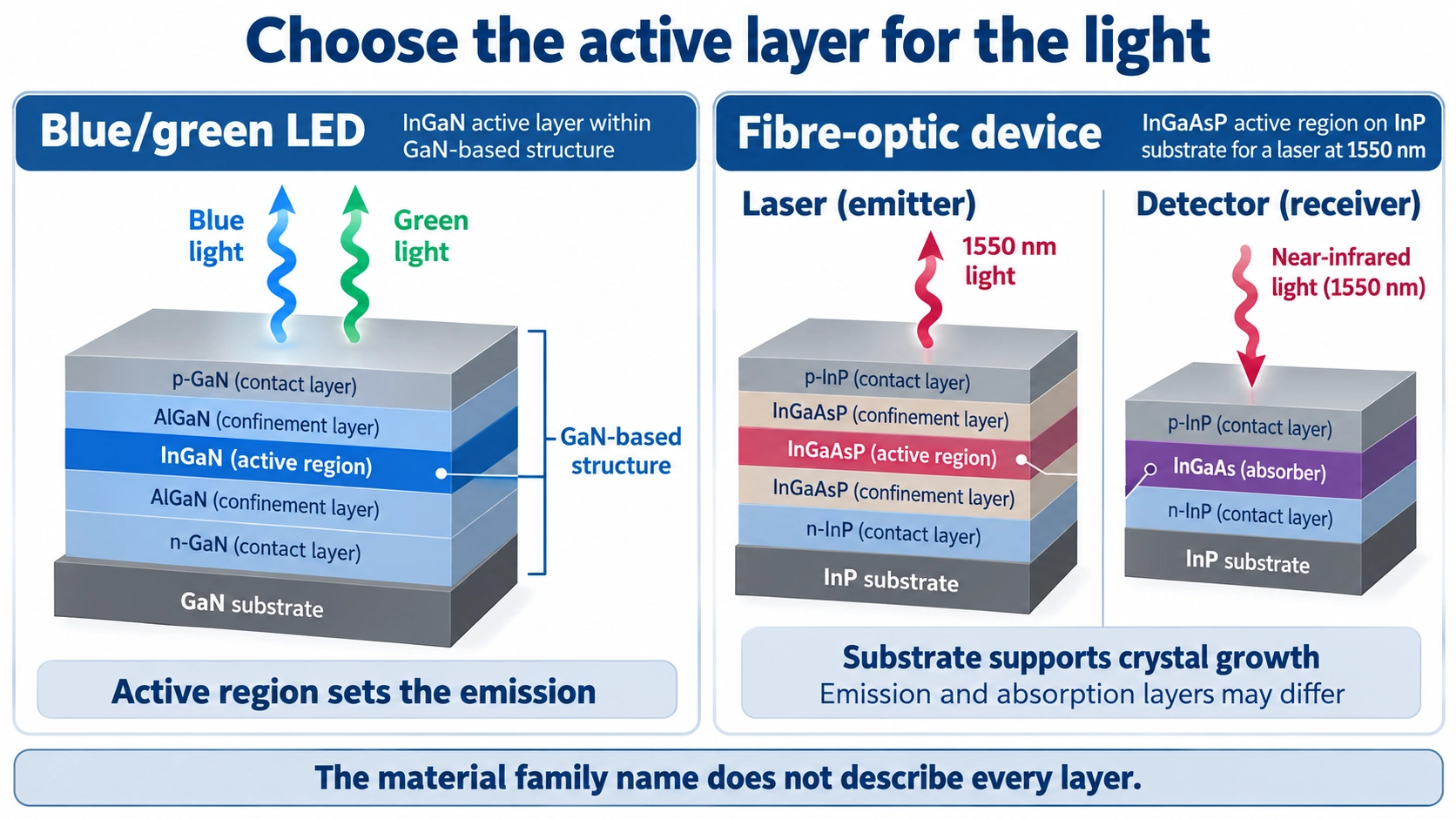
The substrate provides a foundation for crystal growth. The active layer provides the key optical transition. Their lattice compatibility matters because poorly matched layers can develop defects. Calling a device “InP-based” does not mean every layer is pure InP or that pure InP alone emits at the stated telecom wavelength.
A laser also needs optical feedback and gain; choosing a band gap is not enough to make a complete laser. Electrical injection, confinement, heat removal and coupling light into a fibre must all work together.
RF: amplify the signal without losing the information
RF means radio frequency. A mobile transmitter starts with a carefully modulated signal and uses energy from a power supply to produce a stronger RF output. The amplifier does not create useful output energy from the input signal alone.
At high frequency, carrier transport, parasitic capacitances and resistances all matter. At substantial output power, voltage capability and heat removal also matter. Linearity is important because unwanted distortion can corrupt the transmitted information or interfere with neighbouring channels.
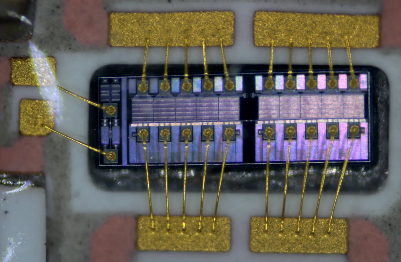
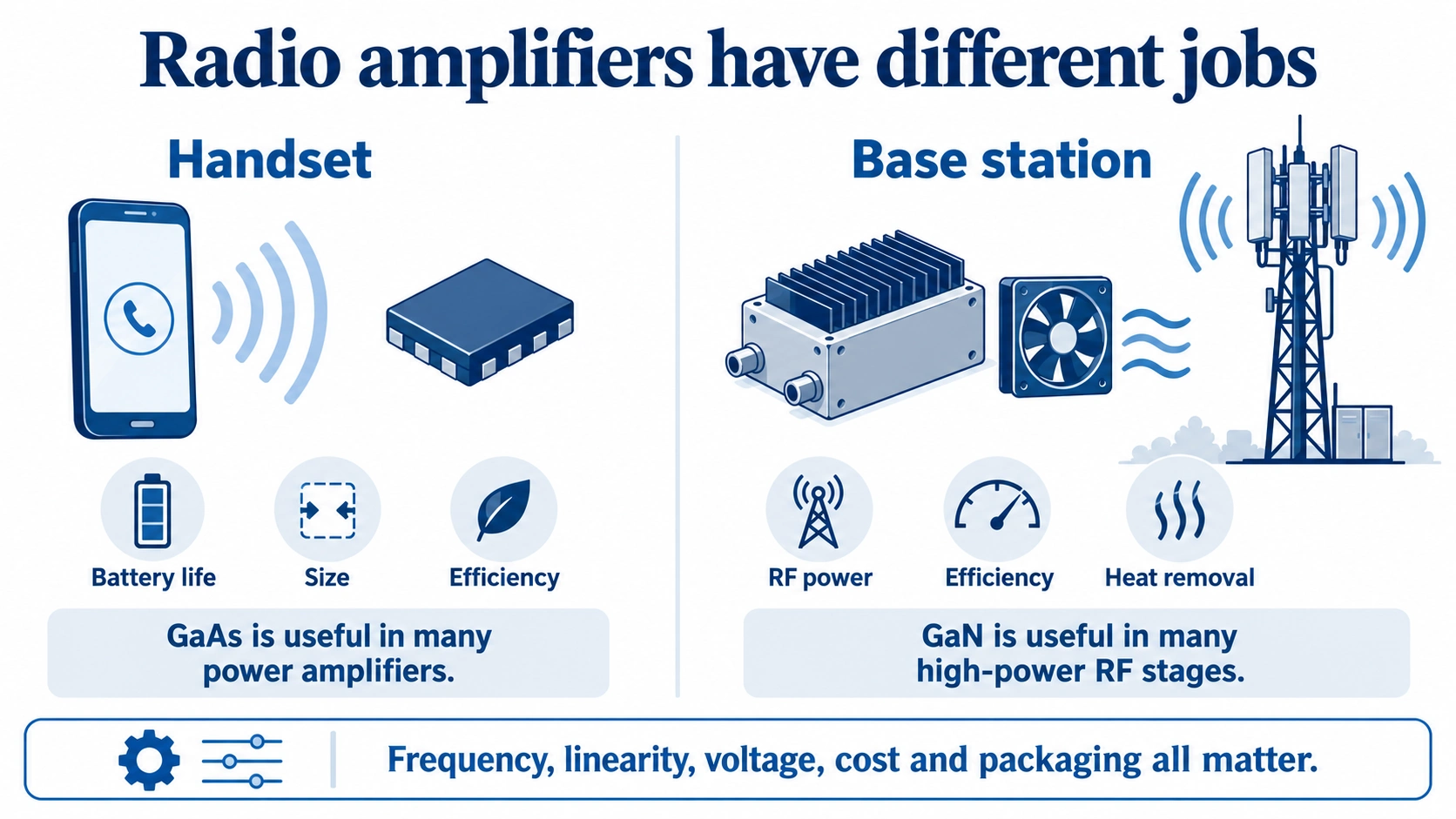
GaAs in a handset; GaN in a high-power RF stage
GaAs has useful electron-transport properties and a long history in compact RF devices. GaAs heterojunction bipolar transistors, or HBTs, are useful in many handset power amplifiers. The choice involves efficiency, linearity, integration and the available battery supply, not mobility alone. [19]
GaN combines useful high-frequency structures with high-field capability. A GaN-on-SiC RF device uses GaN in the electrically active layers and SiC as a supporting substrate with useful thermal properties. This is a different role for SiC from the active SiC MOSFET in a traction inverter. [20]
What makes a HEMT different?
A high-electron-mobility transistor, or HEMT, uses a heterostructure: layers of different semiconductors. In an AlGaN/GaN example, the interface conditions, including polarisation, support a thin electron channel on the GaN side of the boundary. This is called a two-dimensional electron gas, or 2DEG. [13]
“Two-dimensional” describes confinement: electrons are restricted across the thin direction while moving along the interface. It does not mean electrons become flat objects, and “gas” does not mean the solid contains a pocket of air.
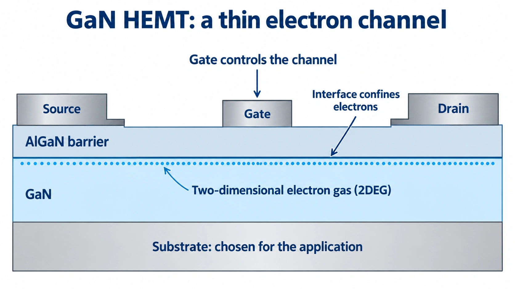
This structure can provide a dense conducting channel without relying on heavy intentional doping of the channel itself. Scattering does not disappear; crystal quality, interfaces and heating still affect transport. The gate controls the channel, while source and drain provide electrical access. [13]
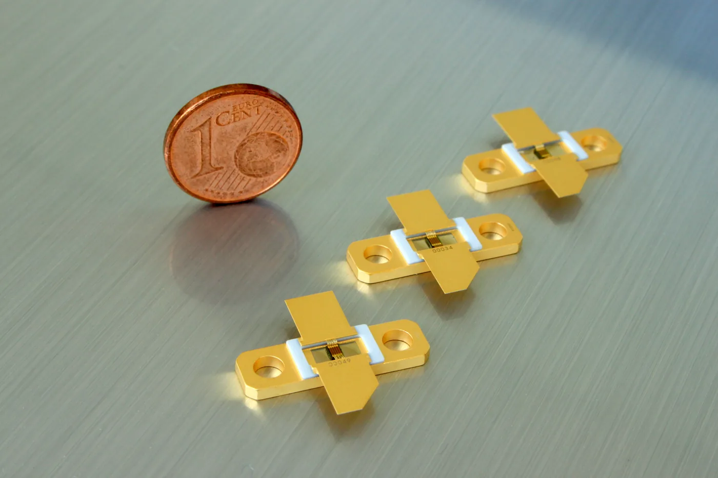
A GaN LED, a GaN power transistor and a GaN RF transistor are not the same component repurposed three times. They use different layer structures and different operating principles to exploit the material family.
A material guide you can reason from
Instead of memorising “material X goes in product Y”, connect the requirement to the property and then to the structure.
| Material or family | Useful strengths | Representative roles and limits |
|---|---|---|
| Silicon, Si | Controlled interfaces, mature integration and large-wafer manufacturing | Logic, memory, analogue, imaging, MEMS and many power devices; not an efficient conventional visible emitter |
| 4H-SiC | High critical electric field and useful thermal properties | High-voltage power switches, including traction; processing, interfaces and cost still matter |
| GaN-based systems | High-field capability and engineered heterostructures | Power HEMTs, RF stages and, with suitable active layers, LEDs; each uses a different structure |
| GaAs-based systems | Useful electron transport and direct-gap optical behaviour | RF devices and selected emitters; not a simple replacement for dense silicon logic |
| InP-based systems | Compatible optical layer systems for near-infrared devices | Lasers and detectors for optical communication; substrate and active layer must be distinguished |
Use three questions when you meet an unfamiliar device:
- What is the useful output? A logic state, stored data, controlled motor current, a measured signal or light?
- What is the limiting problem? Leakage, noise, poor emission, voltage stress, heat, slow transport or cost?
- Which material-and-structure combination addresses that problem? Look for the active layer, the channel, the blocking region and the interfaces.
This way of thinking also prevents overclaiming. A larger band gap does not make a material better at every job. Faster carriers do not automatically make a cheaper processor. A lower device loss does not give the same percentage improvement in an entire vehicle.
Different jobs require different fabrication priorities
| Product | Structures that matter | Particular manufacturing demands |
|---|---|---|
| Leading logic | Small, controllable transistors and dense wiring | Fine lithography, precise etching, gate stacks and interconnect |
| DRAM | Small access devices and sufficient storage capacitance | Deep structures, conformal films, low leakage and sensing consistency |
| 3D NAND | Many word-line levels around vertical channels | Repeated deposition, high-aspect-ratio etching and reliable storage films |
| Analogue IC | Matched devices, precision passives and suitable voltage capability | Process stability, characterisation, isolation and calibration |
| SiC power device | A high-quality crystal, blocking region, channel and contacts | Epitaxy, implantation, high-temperature processing and interface control |
| GaN HEMT | Engineered heterostructure and controlled electron channel | Epitaxial quality, gate and contact design, buffers and field management |
| Image sensor | Low-noise photodiodes and a clear optical path | Surface quality, thinning, bonding and readout integration |
| MEMS | Released mechanical structures and sensing electrodes | Deep etching, stress control, release and protective packaging |
| LED or laser | Optical active region and carrier confinement | Composition control, epitaxy, contacts and thermal management |
Some of the most useful products rely on well-established geometries; others push fine patterning or deep vertical structures. Stacking separate dies belongs to packaging and integration, while making the devices on each die belongs to front-end fabrication. The boundaries connect, but the processes are not interchangeable.
In the next lesson, Introduction 1-3, we turn to semiconductors for AI: why GPUs and HBM matter, and why data movement, heat and power are struggling to keep pace with computation. Introduction 1-4 then follows the manufacturing chain itself: design, wafer processing, assembly and testing, and the companies that supply materials, equipment and production services.
Check your understanding
Are “logic” and “SiC” two alternatives in the same classification?
Show answer
No. Logic describes a function; SiC describes a material. A material can serve several functions, and a function can use several materials.
Why does silicon remain useful for logic even when another material has higher electron mobility?
Show answer
Dense logic needs controllable interfaces, low leakage, complementary devices, reproducibility, interconnect and economical manufacturing. Mobility alone does not meet those requirements.
Why does DRAM need refresh?
Show answer
Stored charge leaks away. Refresh restores the information before the electrical distinction becomes unreliable.
A QLC NAND cell stores four bits. How many distinguishable states are required?
Show answer
Sixteen, because 2 to the power of four is 16. More states demand finer discrimination and robust error management.
How does 3D NAND differ from HBM stacking?
Show answer
3D NAND forms cells through many levels within a die. HBM stacks separate DRAM dies and connects them to provide a wide data path.
Why might an analogue circuit deliberately use larger devices or an established process?
Show answer
Matching, noise, voltage headroom, stability and cost can matter more than maximum density. The best choice depends on the circuit.
Where is the traction inverter in an EV, and what does it do?
Show answer
Between battery and motor. It controls power from the DC battery into the motor phases and can manage the return of energy during regenerative braking.
Is the inverter switching frequency the same as the motor's mechanical speed?
Show answer
No. Switching frequency, electrical field frequency and mechanical rotation are distinct and are related through the controller and motor design.
What three operating situations explain the value of a SiC power switch?
Show answer
Blocking high voltage while off, carrying current with low loss while on, and changing state with manageable switching energy.
If inverter losses fall from four units to two out of a 100-unit input, what happens to output energy?
Show answer
It rises from 96 to 98 units in that hypothetical example. The loss halves; the whole vehicle's energy use does not halve.
Why can a variable-speed pump save energy even without changing from silicon to SiC?
Show answer
Matching motor operation to the required flow can reduce the mechanical energy demand. Reducing converter losses is a separate benefit.
Why does back illumination help a camera pixel?
Show answer
Light reaches the photosensitive silicon before the wiring. This can improve the optical path; readout noise, collection and other design details still matter.
Why distinguish an InP substrate from an optical active layer?
Show answer
The substrate supports crystal growth, while another composition may provide the required emission or absorption wavelength. The family name does not specify every layer.
Does a GaN-on-SiC RF amplifier use SiC in exactly the same way as a SiC traction MOSFET?
Show answer
No. In the RF example, SiC serves as a substrate supporting the GaN-based active structure. In the traction MOSFET, SiC is the active semiconductor material of the power device.
A short glossary
- Logic
- Circuits that represent and combine electrical states to perform operations.
- SoC
- System-on-chip; several functional blocks integrated within one chip.
- DRAM
- Volatile memory commonly using a transistor and capacitor per cell, with refresh.
- NAND flash
- Non-volatile memory read through stored-charge-dependent threshold states.
- Threshold voltage
- A device operating parameter describing the onset of a specified conduction condition.
- Tunnelling
- A quantum process allowing transmission through an energy barrier.
- HBM
- High-bandwidth memory, using connected stacks of DRAM dies near a processor.
- Analogue
- Describing continuously varying electrical signals and the circuits that handle them.
- ADC
- Analogue-to-digital converter.
- Traction inverter
- A converter controlling electrical power between a vehicle's DC supply and traction motor.
- Three-phase
- Three related electrical phases used to deliver power and establish rotating fields.
- PWM
- Pulse-width modulation; control by adjusting the duration of switching states.
- Regenerative braking
- Recovering part of a moving system's energy electrically during deceleration.
- Conduction loss
- Electrical energy lost while a device carries current.
- Switching loss
- Energy lost during switching and associated commutation processes.
- Drift region
- A power-device region designed to support blocking voltage and conduct in the on-state.
- Critical electric field
- A representative limiting field associated with breakdown in a material or structure.
- IGBT
- Insulated-gate bipolar transistor, combining gate control with bipolar conduction.
- Wide-band-gap
- Describing materials such as SiC and GaN with larger gaps than silicon.
- Epitaxy
- Growth of a crystalline layer with an orientation related to the underlying crystal.
- Active layer
- The layer or region carrying out the device's central electrical or optical function.
- Substrate
- The supporting material on which layers or devices are formed.
- MEMS
- Microelectromechanical systems, containing fabricated mechanical structures.
- HEMT
- High-electron-mobility transistor, using an engineered semiconductor heterostructure.
- 2DEG
- Two-dimensional electron gas; a conducting electron population confined across a thin direction.
- RF
- Radio frequency; the signal regime used in radio communication and related systems.
Sources and scope
The references support the material properties, structures and examples used here. The English edition reorganises the explanation for an English-speaking reader. Worked calculations state their assumptions. Illustrations are learning models and are not to scale. Device performance depends on operating point and complete system design; material parameters alone do not determine product efficiency.
- WSTS — Spring 2026 forecast: product categories — Read source
- Intel — High-k and Metal Gate Transistor Research — Read source
- Texas Instruments — CMOS Power Consumption and Cpd Calculation — Read source
- Samsung Semiconductor — Semiconductor glossary: DRAM — Read source
- KOKUSAI ELECTRIC — IR Day 2024: 3D NAND structure example, page 25 (Japanese) — Read source
- DENSO — Power Control Unit — Read source
- Mitsubishi Electric — SiC Lecture Series 4: Physical properties of SiC — Read source
- Toshiba — Features of SiC MOSFETs — Read source
- Texas Instruments — Reducing Power Loss and Thermal Dissipation in SiC Traction Inverters — Read source
- DENSO — DENSO Develops Its First Inverter Using SiC Power Semiconductors, 31 March 2023 — Read source
- Mitsubishi Electric — Inverter Basics — Read source
- Mitsubishi Electric — High Voltage SiC Power Modules — Read source
- Infineon — GaN HEMT Structure: Architecture, Physics and Operation — Read source
- Sony Semiconductor Solutions — Common Technology of Image Sensors — Read source
- Analog Devices — MEMS Gyroscope Provides Precision Inertial Sensing — Read source
- Nobel Prize — The Nobel Prize in Physics 2014 — Read source
- Journal of Semiconductors — Fabrication and optimization of 1.55-µm InGaAsP/InP high-power semiconductor diode laser — Read source
- Hamamatsu Photonics — Compound opto-semiconductor photosensors — Read source
- Nisshinbo Micro Devices — History of GaAs semiconductor products, part 1 (Japanese) — Read source
- MACOM — WGC18630: GaN-on-SiC RF device — Read source
English edition written and reviewed on 31 October 2026. Product examples are dated examples, not claims about every current model. Worked numbers are illustrative unless explicitly attributed.
Original explanatory illustrations generated with OpenAI Image Gen for this English edition. Third-party photographs retain their stated licences; image credits accompany each photograph.