Key Findings
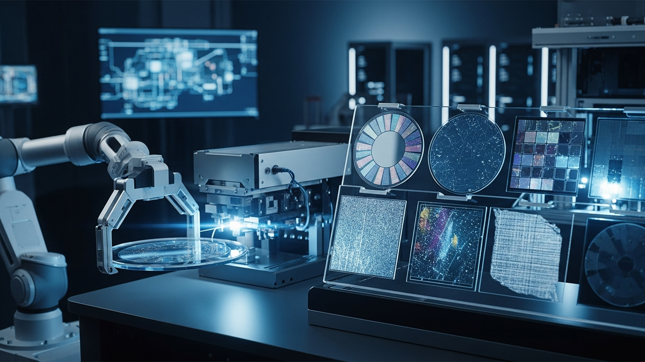
Germany-based planoptik ag is enhancing its offerings of customized glass wafers and panels specifically tailored for MEMS (Micro-Electro-Mechanical Systems) devices and photonic applications. These products are essential solutions within advanced wafer-level packaging (WLP) processes, providing critical protection, encapsulation, and long-term maintenance of performance and reliability for delicate devices against external environments.
Technical Details
The glass wafers and panels provided by planoptik ag are produced using high-precision manufacturing techniques and stringent quality control. Key features include:
- Precise Dimensional Accuracy and Surface Flatness: Packaging of MEMS and photonic devices demands micron-level precision for alignment. planoptik’s glass products meet this requirement with exceptionally high dimensional accuracy and surface flatness.
- Diverse Glass Materials and Thicknesses: A variety of materials and thicknesses are available, such as low thermal expansion glass, high-transmission glass, or specific wavelength-blocking glass, depending on the application’s specific requirements.
- Optimized Optical Properties: For photonic applications, designs are implemented to ensure high optical transmission in specific wavelength ranges and to minimize stray light. Glass cap wafers for optical sensors are optimized to protect the sensor from external contamination and damage while efficiently allowing necessary light signals to pass through.
- High Chemical and Mechanical Durability: Products exhibit high chemical stability and mechanical strength to withstand harsh operating environments and manufacturing processes.
These glass products are utilized in the packaging of devices such as optical switches, optical sensor arrays, micromirrors, and microfluidic chips, contributing to the functional protection and performance maximization of the devices.
Background & Context
In the semiconductor industry, there is a constant demand for device miniaturization, enhanced performance, and cost reduction. Wafer-Level Packaging (WLP) is a crucial technology for meeting these demands. MEMS and photonics devices, due to their specialized functionalities, face unique challenges distinct from traditional IC packaging. Specifically, the precise guiding of optical signals, environmental protection, and thermal compatibility between disparate materials are addressed by glass-based packaging solutions. Specialized companies like planoptik ag cater to these niche yet highly advanced market needs, supporting technological innovation across the entire semiconductor ecosystem.
Strategic Significance & Outlook
The application scope of MEMS and photonic devices is continuously expanding into fields such as autonomous driving, AR/VR, IoT sensors, advanced medical devices, and data communications. Innovation in these areas will further drive demand for high-performance and reliable WLP solutions. The customized glass wafers and panels offered by planoptik ag are expected to play an indispensable role in the mass production and performance optimization of these next-generation devices. Through continuous R&D and close collaboration with customers, the company is poised to adapt to market evolution and expand the frontiers of WLP technology.
Source: https://www.planoptik.com/en/products/wafer_level_packaging/
Get our weekly technology intelligence — free
Receive an infographic that lets you judge at a glance whether each field’s analysis report is worth reading.
Subscribe Free — Weekly Tech Intelligence
By subscribing, you’ll receive Troy-Technical’s weekly technology intelligence newsletter.
- Your email and selected fields are used only to deliver the newsletter.
- We never share your information with third parties.
- You can unsubscribe anytime via the link in each email.
See our Privacy Policy for details.
Takes about a minute · Unsubscribe anytime





Comments