Key Findings
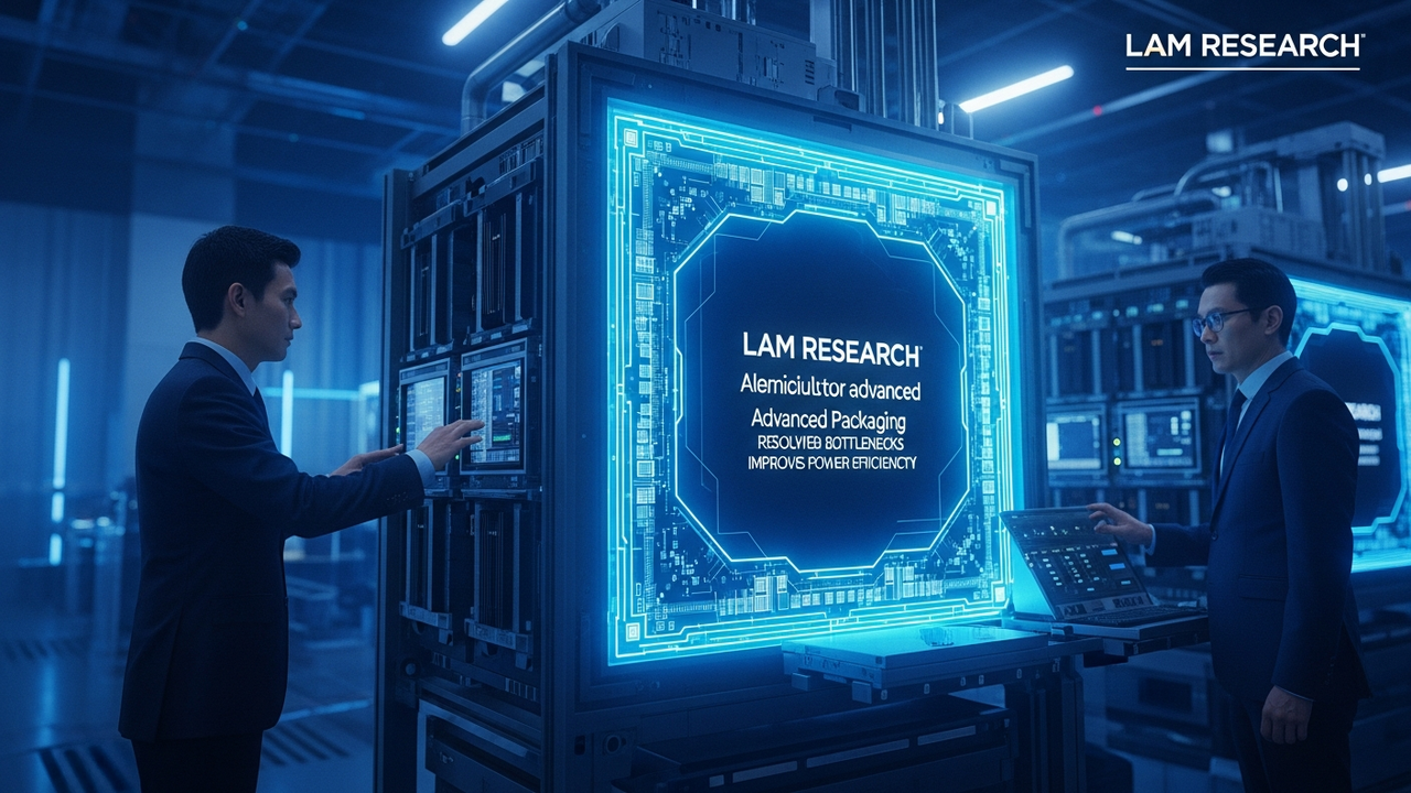
Lam Research is introducing advanced packaging technologies as the new frontier for semiconductor scaling, crucial for meeting the explosive demand from artificial intelligence (AI). The company emphasizes that chiplet technology and the transition to panel-based packaging are key enablers for dramatically boosting AI performance.
Technical Details
According to Audrey Charles, Lam Research’s Senior Vice President of Corporate Strategy and Advanced Packaging, AI growth is outpacing traditional semiconductor process scaling, making advanced packaging indispensable for bridging this gap. Chiplet technology involves integrating multiple independent dies (chiplets) within a single package, allowing them to function as a unified system. This approach significantly reduces data transmission bottlenecks, dramatically increases memory bandwidth through integration with High-Bandwidth Memory (HBM), and improves overall power efficiency. These characteristics directly address the immense data processing power and low power consumption required by AI workloads.
Furthermore, the industry is shifting from conventional wafer-based packaging to larger panel-based packaging formats to enhance manufacturing efficiency and reduce costs. To support this transformation, Lam Research has established its Salzburg Panel Center of Excellence, building large-scale advanced packaging manufacturing capabilities at the panel level. Panel-based processes enable the simultaneous processing of a much greater number of chips, offering potential cost reductions compared to wafer-based methods, especially in fan-out packaging.
Background & Context
The semiconductor industry is encountering the physical limits of Moore’s Law, where scaling transistor density alone is insufficient to meet the performance demands of AI applications. Consequently, advanced packaging, which improves inter-chip connectivity, memory bandwidth, and power delivery, has emerged as a primary means to achieve next-generation performance gains. AI processors, in particular, necessitate the efficient and high-density integration of GPUs and HBM, driving the need for sophisticated packaging technologies.
Strategic Significance & Outlook
Lam Research views panel-based packaging technology as a foundational element for future growth in the AI and high-performance computing (HPC) markets. The company’s technologies are expected to provide the scalability and efficiency required for increasingly complex AI architectures, accelerating innovation across the semiconductor industry. This strategic shift will likely impact a broad supply chain, including materials suppliers and equipment manufacturers, creating new business opportunities and reshaping the competitive landscape.
Source: https://newsroom.lamresearch.com/advanced-packaging-for-ai-semiconductor-scaling
Get our weekly technology intelligence — free
Receive an infographic that lets you judge at a glance whether each field’s analysis report is worth reading.
Subscribe Free — Weekly Tech Intelligence
By subscribing, you’ll receive Troy-Technical’s weekly technology intelligence newsletter.
- Your email and selected fields are used only to deliver the newsletter.
- We never share your information with third parties.
- You can unsubscribe anytime via the link in each email.
See our Privacy Policy for details.
Takes about a minute · Unsubscribe anytime









Comments