TECHNOLOGY EXPLAINER
Atomic Layer Deposition (ALD)
— stack reactions that stop when saturated, and set thickness by counting
ALD builds a film by alternating two gases and repeating reactions that stop once the surface is saturated. The growth per cycle (GPC) is on the order of 0.1 nm, so thickness is set by the number of cycles, and even deep three-dimensional structures can be coated uniformly. The price is time: in a laboratory example where one cycle takes seconds, a 5 nm film takes more than half an hour. This article sets out the mechanism, precursors and reactants, thermal and plasma ALD, area-selective ALD, applications and the time problem, keeping the origin of each number clear.
Sources: original studies by Kim, Baishya, Gordon, Knoops, Rhee and Poodt; Mistry’s original abstract; and ASM’s own technical and annual reports. Condition-specific results are distinguished from illustrative calculations. Updated 17 October 2026.
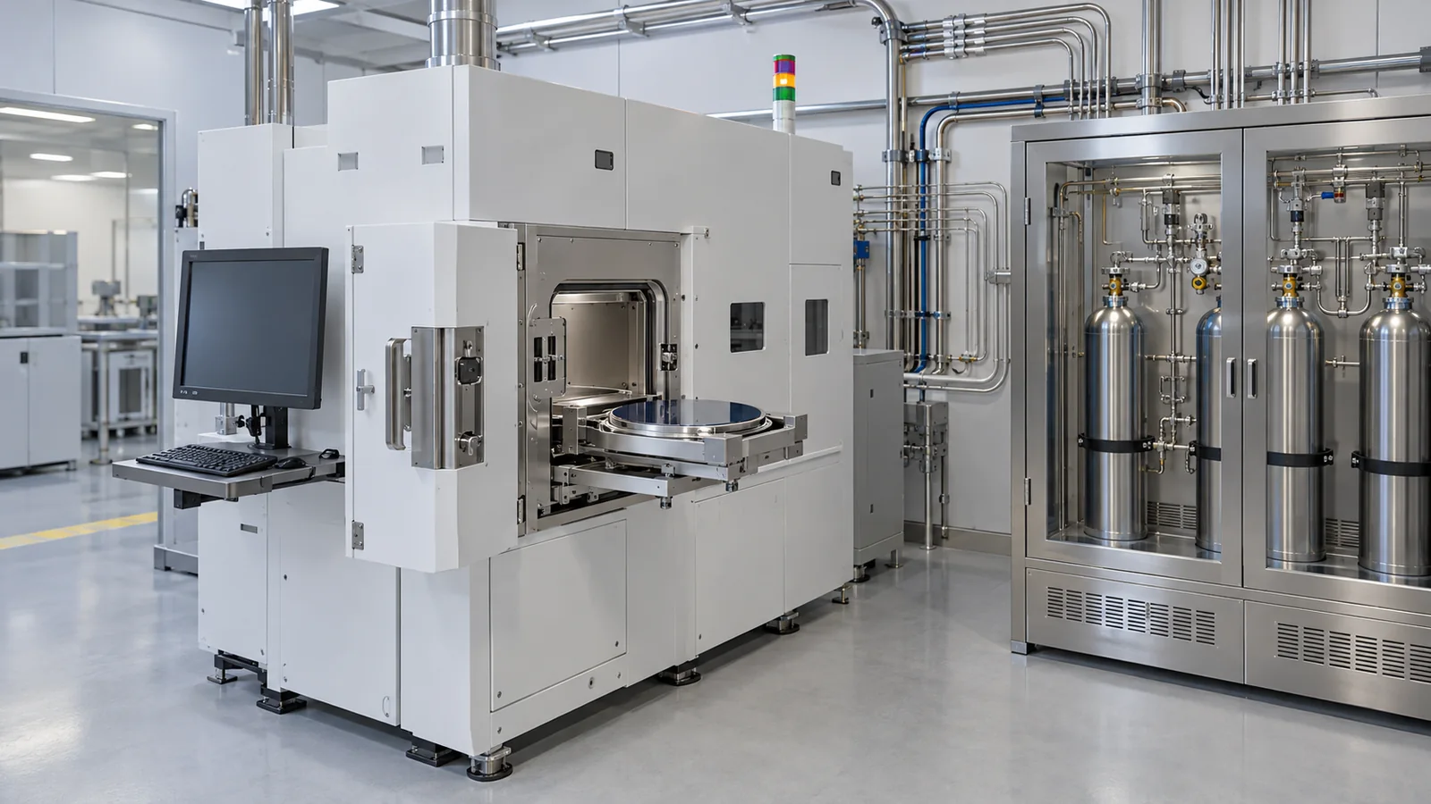
- What atomic layer deposition (ALD) is (the short version)
- Self-limiting reactions and the cycle
- Thickness set by the number of cycles: the ALD window
- Precursors and reactants: what is combined, and how
- Thermal ALD and plasma ALD
- Coating three-dimensional structures
- Area-selective ALD
- Applications: high-k gate dielectrics, DRAM, spacers, barrier layers
- The throughput problem: our calculation
- How to read the numbers: keep laboratory, manufacturer's outlook and calculation apart
- Limits and what we could not confirm
- How to read evaluations and standards
- Glossary
- References (primary sources)
- Claim-to-source audit
Sourced = a statement in published material (link given)
Our calculation = a figure this article derived, with the assumptions spelled out
Not yet confirmed = a plan or target with no confirmed track record
Structural readings and materials-design interpretations are marked separately as Commentary.
Growth rates and film properties are written together with what was measured (method), which tool and conditions (temperature, pulses, substrate) and at what level (laboratory or production). Company statements are labelled as the manufacturer's, and market-size estimates by research firms are not used.
This is an explainer on the principles and evaluation of film deposition in semiconductor manufacturing. Precursors (gases and vapours) include toxic, pyrophoric and corrosive substances, and their handling is governed by the supplier's safety data sheets (SDS) and the law. This article gives no handling advice and does not rank any company, tool or country.
1. What atomic layer deposition (ALD) is (the short version)
ALD is a method that supplies two reactants to a surface in turn and builds a film in units close to an atomic layer, using the fact that each reaction saturates and stops on the surface. If etching is "removing", this is "stacking uniformly".
- Definition: ASM describes separated precursor/reactant exposures with surface saturation to grow a film [Ref. 6]. Our explanation below does not mean that every cycle deposits exactly one atomic layer.
- Breadth of use: ASM International lists high-k metal gates, spacer dielectrics for patterning, MIM capacitors, gate spacers and high-aspect-ratio gap-fill, among others (the manufacturer's description)Sourced
- 2025 was the ramp year for GAA (gate-all-around): in its 2025 annual report ASM says the 3D structure of GAA and the need for tighter control call for additional ALD steps (the manufacturer's statement)Sourced
ALD sets thickness by counting cycles, so thickness can be controlled precisely, but that costs time. Al2O3 (TMA/water) grows at about 1.1 Å per cycle and TiN (TiCl4/NH3) at about 0.47 Å per cycle, both laboratory reportsSourced. On the laboratory tool of the latter, one cycle takes 19.5 s, so a 5 nm TiN film takes about 35 minutesOur calculation. Combining precision with speed is being worked on in both tools and materials.
In this series, our explainer on lithography and EUV touched on the spacer films of multiple patterning, and our explainer on resists and photomasks touched on dry resists (films made by deposition). ALD is what actually lays down such films. The next article, on etching, covers the other side: removing what ALD deposits.
2. Self-limiting reactions and the cycle
The basic time-separated sequence is precursor, purge, reactant, purge [Ref. 6]. Self-limiting means the surface reaction saturates under suitable conditions, not that any temperature, dose or geometry guarantees saturation. Kim et al.’s TMA/water experiment used 1, 40, 2 and 40 seconds respectively [Ref. 3].
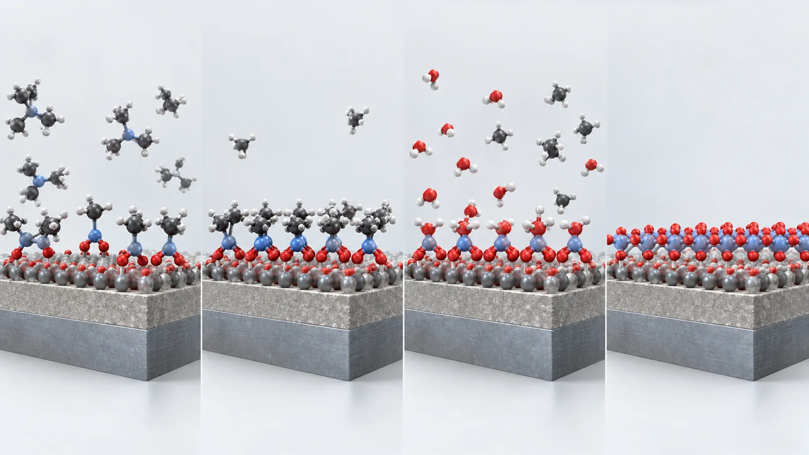
Shapes, colors and dimensions are illustrative. Consult the original schematic below for exact values and label correspondence.
View the original SVG schematic and exact annotations
Reading guide: blue represents precursor and red represents reactant. Repeat precursor, purge, reactant, purge; growth need not equal one atomic layer. Basic sequence: ASM [Ref. 6]; experimental pulse timing: Kim et al. [Ref. 3].
Original schematic: conceptual four-step sequence following ASM [Ref. 6]. Counts, placement and coverage are not measured data.
Check separated exposures and surface saturation separately. GPC is a measured quantity for a material and recipe. Kim et al.’s Al2O3 gave 0.9–1.1 Å/cycle, not an automatic one-atomic-layer increment [Ref. 3]. Our process-reading guidance is to check sufficient purge and saturation.
3. Thickness set by the number of cycles: the ALD window
When GPC is constant, thickness ≈ cycles × GPC. Different initial nucleation can invalidate simple proportionality. Here, the ALD window refers to the near-constant growth range in Kim et al.’s TMA/water experiment [Ref. 3], not a temperature range transferable to other materials.
Kim et al. (2022, peer-reviewed) grew Al2O3 from TMA and water in a traveling-wave-type ALD reactor (80 to 250 °C) and took the GPC from the slope of film thickness measured by spectroscopic ellipsometry against the number of cycles. GPC rose from about 0.9 Å per cycle at 80 °C to a constant about 1.1 Å per cycle at 150–250 °C in the tested range, so 150–250 °C in the tested range was the ALD window (purge time fixed at 40 s)Sourced. The authors attribute the lower GPC below 150 °C to a slower reaction caused by the thermal activation barrier for removing the ligand (CH3)Sourced.
Baishya et al. (2026, peer-reviewed) grew TiN from TiCl4 and NH3 at 400 °C. One cycle was a 0.5 s TiCl4 pulse, 4 s purge, 2.5 s NH3 pulse, 5 s purge, 2.5 s NH3 pulse and 5 s purge, giving about 0.047 nm per cycle. 100, 200, 300 and 400 cycles gave 4.7, 9.4, 14.1 and 18.8 nm (a laboratory ALD tool)Sourced.
From the laboratory GPC values, the number of cycles needed for a 10 nm filmOur calculation.
- Al2O3 (1.1 Å per cycle): 10 nm ÷ 0.11 nm = about 91 cycles
- TiN (0.047 nm per cycle): 10 nm ÷ 0.047 nm = about 213 cycles. The 4.7 nm TiN is 100 cycles
- Step of thickness: the thickness added per cycle is a guide to the smallest step (about 0.11 nm for Al2O3, about 0.047 nm for TiN)
Assumptions and limits: GPC changes with temperature, precursor, reactor and substrate state, and both values used here are laboratory-tool reports. The GPC of production tools, and cases where thickness is not proportional to cycles in early growth (nucleation), are not included.
4. Precursors and reactants: what is combined, and how
The film material is set by the combination of a precursor (the molecule that carries the metal or other element) and a reactant (a molecule or plasma that supplies oxygen, nitrogen and so on). Here are reported examples, with their conditions.
| Film | Precursor | Reactant | Conditions and measured values (level) | Source |
|---|---|---|---|---|
| Al2O3 | Trimethylaluminum (TMA) | Water | 80 to 250 °C. GPC about 0.9 Å (80 °C) and about 1.1 Å (150–250 °C in the tested range). Spectroscopic ellipsometry (laboratory) | Kim et al. (2022) |
| HfO2 | Hafnium dimethylamide | Water | Fully conformal coverage of holes with aspect ratio 43 (laboratory) | Gordon et al. (2003) |
| TiN | TiCl4 (a chloride) | NH3 | 400 °C. About 0.047 nm per cycle (laboratory tool) | Baishya et al. (2026) |
| SiNx (PEALD) | BTBAS | N2 plasma | The original study examined room temperature to 500 °C and reported good film quality at table temperatures of 300–500 °C. Not a universal SiN process recommendation. | Knoops et al. (2015) [Ref. 1] |
Each row is a condition-specific original-study example. Different tools, substrates and measurements prevent ranking materials or methods by temperature or GPC alone. The SiN description is limited to the original abstract of Knoops et al.
A precursor must meet at least these conditions at once (this article's commentary): (1) enough vapour pressure to be delivered; (2) reactive with the surface at the reaction temperature but not decomposing at the supply temperature (this sets the upper edge of the ALD window); and (3) by-products that leave as gas and do not stay on the surface. The kind of ligand (chloride, organometallic) changes the impurities likely to remain. Kim et al. report that in Al2O3, the lower the growth temperature, the more carbon impurity and oxygen defects and the lower the dielectric breakdown strength. The film grown at 150 °C had a breakdown field of about 8.3 MV/cmSourced (measured under that paper's conditions; laboratory samples). Baishya et al. also report that ultrathin TiN oxidizes at the surface in air, and that the oxygen concentration measured by XPS is higher for thinner films (about 30% at 4.7 nm, about 18% at 18.8 nm). The authors explain that XPS probes the top 5 to 10 nm, so the oxidized layer weighs more in thin filmsSourced. So in evaluating ultrathin films, the film itself and the surface and interface layers must be considered separately.
From Baishya et al.'s four-point-probe sheet resistance (on glass, before the additional air-exposure test) and film thickness we calculate resistivity = sheet resistance × thicknessOur calculation.
- 100 cycles (4.7 nm): 222.3 kΩ/sq × 4.7 nm = about 100,000 µΩ·cm
- 200 cycles (9.4 nm): 2.5 kΩ/sq → about 2,350 µΩ·cm; 300 cycles (14.1 nm): 519 Ω/sq → about 730 µΩ·cm
- 400 cycles (18.8 nm): 287 Ω/sq → about 540 µΩ·cm (the same as the authors' value)
Assumptions and limits: the sheet resistance is the paper's value (glass substrate, before air exposure) and the thickness is the nominal one calculated from the growth rate. That the 4.7 nm value is about 200 times larger is consistent with continuity, surface oxidation and grain boundaries mattering more in thin films, but this article did not check the breakdown. The performance of TiN, used for barriers and electrodes, changes greatly with the thickness used.
5. Thermal ALD and plasma ALD
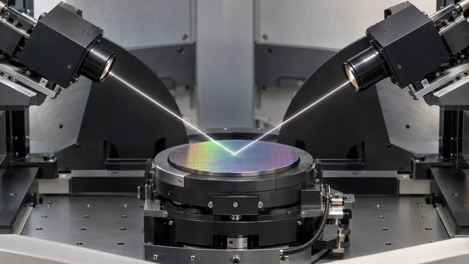
Thermal and plasma ALD differ in how reaction energy is supplied. ASM describes PEALD for low-thermal-budget applications [Ref. 6]. We do not generalise thermal ALD to 150–350 °C or require every PEALD process to stay below 500 °C. The table is a reading checklist, not a ranking.
| Item | Thermal ALD | Plasma ALD |
|---|---|---|
| Reaction energy | Check whether thermal reaction is sufficient | Check plasma source and exposure |
| Temperature | Read the material, precursors and substrate conditions | Read table temperature and plasma exposure |
| Precursor suitability | Does the target reaction saturate? | Does the recipe yield the required film quality? |
| Deep structures | Check dose and pressure × exposure time | Check measured coverage in the target geometry |
| Underlying layers | Measure thermal-history and interface effects | Measure interface effects after thermal/plasma exposure |
This table is our editorial checklist. Consult ASM for low thermal budget [Ref. 6], Knoops et al. for SiN temperature/exposure and film quality [Ref. 1], and Gordon et al.’s model for delivery into deep holes [Ref. 5]. The table is not one comparative experiment.
ASM explains that PEALD enables low-thermal-budget applicationsSourced. What a transistor already has (dopant profiles, metals, low-k films, organic films) is sensitive to high temperature, so the later a film is laid down, the lower the temperature it needs (this article's commentary). The plasma, on the other hand, brings a trade-off between conformality and damage. Finding conditions that deposit at low temperature, uniformly into deep structures, and without damage is the heart of PEALD development (commentary).
6. Coating three-dimensional structures
One of ALD's greatest strengths is that it can coat evenly to the bottom of deep holes and trenches. Gordon et al. (2003, peer-reviewed) derived two conditions for uniform coating using self-limiting reactions: (1) a certain minimum amount of vapour must be supplied, and (2) a certain minimum product of vapour pressure and exposure time at the hole entrance. The theory agreed well with data in which HfO2 from hafnium dimethylamide and water coated holes of aspect ratio 43 completely conformallySourced.

Shapes, colors and dimensions are illustrative. Consult the original schematic below for exact values and label correspondence.
View the original SVG schematic and exact annotations
Reading guide and original schematic labels: Coverage of steps and deep holes (conceptual) / Cross-section sketch. Orange is the deposited film. Differences in thickness are exaggerated. / Physical deposition (PVD) / Thick on top, thin on / sidewall and bottom / Chemical vapor deposition / In between; depends / on conditions / Atomic layer deposition / About the same thickness / on top, wall and bottom / Aspect ratio / width / depth / AR = depth ÷ width / deeper means harder to reach / * A concept of ALD's uniform coverage from self-limiting reactions [Ref. 1, 6]; real thickness ratios are not shown. / * Gordon et al. [Ref. 5] report fully conformal HfO2 in holes of aspect ratio 43 using a hafnium amide and water.
Original SVG reference: Conceptual diagram (vector drawing). A schematic that emphasizes the difference in coverage among physical deposition, CVD and ALD [Ref. 1, 5, 6]. It does not show real thickness ratios or shapes.
The time for a precursor to diffuse to the bottom of a deep hole generally scales with the square of the depth (a basic diffusion relation; our assumption)Our calculation.
- If the aspect ratio doubles from 43 to 86, the guide to the required exposure is (86 ÷ 43)² = about 4 times
- From 43 to 100, (100 ÷ 43)² = about 5.4 times
Assumptions and limits: Gordon et al. say they derived "simple scaling laws", but this article did not check the equations themselves. The square law used here is a general guide to the time to diffuse in, and varies with the reaction probability (sticking) and how by-products escape. It shows the direction: deeper structures need longer exposure, which worsens the throughput problem discussed later.
7. Area-selective ALD
Area-selective ALD distinguishes growth and inhibited regions. The diagram is our conceptual explanation of the aim and the need to check unwanted growth, not the workflow of a particular paper. Rhee et al. experimentally distinguished grain boundaries and other regions of a ZrO2 surface [Ref. 7].
Rhee et al. treated ZrO2 grain boundaries with SF6 and inhibited other regions using a ligand from ZrCp(NMe2)3. TEM elemental mapping supported grain-boundary-targeted Al2O3 [Ref. 7]. This is one material and surface-treatment experiment, not a recipe shared by all selective ALD.
When considering correction steps, ask what was removed, whether the intended film remained, and over how many cycles selectivity was measured. These are our evaluation questions, not rules that selectivity depends only on thickness or that every method uses selective etching.
8. Applications: high-k gate dielectrics, DRAM, spacers, barrier layers
(1) High-k gate dielectrics and metal gates
Mistry et al.’s 2007 original abstract reports a 1.0 nm EOT high-k dielectric and dual metal gates in 45 nm logic [Ref. 8]. It does not state the deposition method, so it alone does not prove ALD was used. Our checklist also asks about leakage, interfaces, reliability and subsequent processing, not permittivity alone.
ASM's 2025 annual report says that in advanced transistor structures ALD is concentrated in functional layers such as high-k dielectrics, dipole layers for multi-Vt and work-function metals. It expects these transistor layers to account for about 50% of ALD layers at the 2 nm node and about 60% at the 1.4 nm node (the manufacturer's outlook)Not yet confirmed. It also began shipping its first applications of molybdenum (Mo) ALD at 2 nm, and expects Mo ALD to replace more of the existing metal as dimensions shrink (the manufacturer's outlook)Not yet confirmed. It also states that ALD adoption is growing in MIM capacitors and backside-power architecturesSourced.
(2) The DRAM capacitor
Rhee et al. compared MIM specimens on TiN: 3 nm ZrO2 / two Al2O3 cycles / 3 nm ZrO2, deposited at 250 °C and post-annealed for one minute at 600 °C in N2. ZAZ+F+Cp had 15.5% higher effective permittivity than conventional ZAZ, with similar leakage [Ref. 7]. Means used at least ten measurements per sample after 1.5-IQR outlier removal. This is not a general commercial-DRAM improvement rate.
(3) Spacers
Think of a spacer as a sidewall film. ASM lists gate and patterning spacers as applications [Ref. 6]. Knoops et al. studied how table temperature, exposure and pressure affected SiN film quality with BTBAS/N2 plasma [Ref. 1]. That experiment is not evidence of production at 32/28 nm nodes.
(4) Barrier layers and electrodes
Baishya et al. state that TiN is used as a diffusion barrier in ultra-large-scale integration (ULSI) and as a capacitor electrode in DRAMSourced. To work as a barrier even when extremely thin, the film needs continuity and purity, and as we saw, ultrathin TiN shows strong effects in resistivity and surface oxidation.
For ultrathin films, check continuity, substrate interfaces, impurities and later processing separately. This is our materials-design framework. The TiN thickness, Al2O3 temperature and Rhee stack comparisons are different experiments, not one universal causal law.
Arithmetic note: the following times use unrounded thickness/GPC as a continuous approximation. Real recipes need integer cycles: at least 2 and 5 nm require rounding up to 43 and 107 cycles. At 19.5 s/cycle, those take about 14.0 and 34.8 minutes, excluding handling.
9. The throughput problem: our calculation
Time-separated ALD repeats exposure and purge, so cycle time matters alongside thickness. As an original spatial-ALD example, Poodt et al. (2010) reported Al2O3 for solar-cell surface passivation [Ref. 2]. We use the application and approach confirmed by the public original abstract, not an extrapolation to semiconductor-wafer production throughput.
With TiN's GPC (0.047 nm), the time for 2 nm and 5 nm films for three assumed cycle timesOur calculation.
- Laboratory example (19.5 s per cycle, Baishya et al.): 2 nm (about 43 cycles) takes about 13.8 min and 5 nm (about 106 cycles) about 34.6 min
- Assumed (5 s per cycle): about 3.5 min for 2 nm and about 8.9 min for 5 nm
- Assumed (2 s per cycle): about 1.4 min for 2 nm and about 3.5 min for 5 nm
A guide to the number of chambers: if one chamber processes one wafer at a time and eight chambers must handle 60 wafers per hour, each wafer may occupy a chamber for 8 × 60 min ÷ 60 wafers = 8 min at most. For 2 nm (about 43 cycles), that means a cycle time of about 11 s or lessOur calculation. ASM describes its single-wafer thermal ALD tool Synergis as a high-productivity tool that can be configured with up to four dual chamber modules (eight chambers in all) (the manufacturer's description)Sourced.
Assumptions and limits: 19.5 s per cycle is the total of pulses and purges on a laboratory tool, not a production-tool value. 5 s and 2 s are this article's assumptions, and the real production cycle times could not be confirmed here. Wafer loading, heat-up and chamber cleaning are not included.
Precursor utilisation requires consistent accounting of supply, incorporation into film, and material remaining in exhaust or lines (our framework). It depends on tool, dose and accounting boundary; we adopt no percentage whose original conditions are unverified. Alongside speed and film quality, check exactly what the material balance includes.
Shortening a cycle means shortening pulses and purges. To saturate even with a short pulse, the precursor must adsorb and saturate quickly and desorb quickly in the purge. A low-vapour-pressure precursor makes line temperature control and securing the supply harder (this article's commentary). Together with the fact that deeper structures need longer exposure (Section 6), precursor design bears directly on time per wafer. Using plasma (PEALD), spatial separation and multiple chambers are solutions from the tool side rather than the material side (commentary).
10. How to read the numbers: keep laboratory, manufacturer's outlook and calculation apart
| Number | What it is | Category | Caution |
|---|---|---|---|
| About 1.1 Å/cycle (150–250 °C in the tested range), about 0.9 (80 °C) | Growth rate of TMA/water Al2O3 | Peer-reviewed paper (2022, ellipsometry) | A laboratory traveling-wave reactor. 40 s purge |
| About 0.047 nm/cycle; 19.5 s per cycle | Growth rate and cycle time of TiN from TiCl4/NH3 at 400 °C | Peer-reviewed paper (2026) | A laboratory tool. Not a production cycle time |
| About 100,000 / about 540 µΩ·cm | Resistivity of TiN at 4.7 nm / 18.8 nm (sheet resistance × thickness) | Our calculation (the paper's sheet resistance and nominal thickness) | On glass, before exposure. Breakdown not checked |
| Aspect ratio 43 | The hole coated completely uniformly with HfO2 | Peer-reviewed paper (2003) | Laboratory conditions. Not the same as production structures |
| 15.5% | Relative effective-permittivity increase in grain-boundary-selective ZAZ specimens | Rhee original study | Relative to that study’s reference, not a general commercial-DRAM improvement. |
| EOT 1.0 nm | The high-k gate dielectric first used in volume production at 45 nm | Paper abstract (2007) | The abstract gives no deposition method |
| 50% to 60% | Share of transistor layers in ALD layers (2 nm to 1.4 nm) | Manufacturer's outlook (2025) | Not yet confirmed |
| 13.8, 34.6 min and others | Calculated TiN deposition times | Our calculation | Cycle times other than 19.5 s are assumptions |
11. Limits and what we could not confirm
(1) We could not confirm actual cycle times or growth rates of production tools
The GPC values and cycle time used here are all values from laboratory-tool papers. We found no concrete throughput figures for production ALD tools in the manufacturer's technical material, so we could not confirm them.
(2) We could not confirm how high-k films are deposited in logic
Mistry et al.'s abstract does not state how the high-k gate dielectric was deposited. ASM says its ALD tools (such as Pulsar) are used for high-k metal gates, but whether a particular company's process is ALD could not be confirmed from the primary sources used here.
(3) Precursor safety and regulation are not covered
The safety and environmental regulation of precursors and reactants (pyrophoric organometallics, corrosive halides, toxic gases and so on) is outside the scope of this article. Handling follows the supplier's SDS and the law. Fluorinated gases and regulation are taken up in our explainer on etching.
(4) Atomic layer etching (ALE) and the integration of deposition and etch come in the next article
Combinations of ALD and etching, such as the correction steps of area-selective ALD, will be organized together with atomic layer etching (ALE) in our explainer on etching.
- ALD stacks a film by repeating self-limiting reactions, and thickness is set by cycles × GPCSourced
- Al2O3 (TMA/water) grows at about 1.1 Å per cycle and TiN (TiCl4/NH3) at about 0.047 nm per cycle (both laboratory). 10 nm is about 91 and about 213 cyclesOur calculation
- PEALD is an option for low thermal budget; verify temperature, exposure and film quality for each experiment and tool [Ref. 1, 6].
- Gordon et al.’s HfO2 experiment/model concerns deep-hole coverage [Ref. 5]. Rhee et al.’s grain-boundary experiment concerns selective growth [Ref. 7]. These are different evaluations.
- In ultrathin films, continuity, interfaces and impurities set the values. The resistivity of 4.7 nm TiN is about 200 times that of 18.8 nmOur calculation
- The biggest problem is time. Under laboratory conditions a 5 nm TiN film takes about 35 minutes by our calculation, and production cycle times could not be confirmed
12. How to read evaluations and standards
Before comparing which number is larger, align the basis of comparison in the following order. This is an editorial reading checklist, not a set of test conditions or acceptance limits prescribed by a standard.
- 1. What was measured?
- growth per cycle, thickness uniformity, conformality, impurities and electrical properties. Check the units and whether the result describes a material, component or complete system.
- 2. Under which conditions?
- precursor, temperature, dose, purge, substrate, feature depth and measurement method. Treat results under different conditions as separate results before comparing them.
- 3. The comparison trap
- Reaching a target thickness alone does not prove low defects, insulation or coverage in deep features.
- 4. What does the standard cover?
- Check the identifier, title, edition and scope in the issuing body’s material. Distinguish test methods, safety, interoperability and management requirements. Naming a standard alone does not establish that a test, conformity assessment or certification has been completed.
Keep a comparison note containing the object, units, conditions, sample count and variation, comparator, standard edition and unresolved points. Do not invent numerical conditions or acceptance limits from a public abstract of a standard.
13. Glossary
- ALD
- Atomic layer deposition. Film growth by alternating self-limiting reactions.
- Precursor
- The molecule that carries the film's element (a metal, for example). Examples: TMA, TiCl4.
- Reactant (co-reactant)
- The substance that supplies oxygen, nitrogen and so on by reacting with the precursor: water, NH3, plasma.
- Purge
- The step that removes excess molecules and by-products with inert gas.
- GPC
- Growth per cycle. The film thickness added in one cycle.
- ALD window
- The temperature range in which GPC is nearly constant.
- PEALD
- Plasma-enhanced ALD. Uses plasma in the reactant step.
- Conformal
- Coating evenly, following steps and holes, with uniform thickness.
- Aspect ratio (AR)
- Depth ÷ width of a hole or trench.
- Area-selective ALD
- ALD that grows film only on a chosen material (AS-ALD).
- EPE
- Edge placement error. The displacement of a pattern edge.
- High-k
- An insulating material with a higher permittivity than SiO2, such as HfO2.
- EOT
- Equivalent oxide thickness. The thickness of SiO2 that would give the same capacitance.
- GAA
- Gate-all-around. A structure in which the gate surrounds the channel (nanosheet) on all sides.
- Spatial ALD
- ALD that separates the half-reactions in space instead of using purge steps.
14. References (primary sources)
- Knoops H.C.M. et al. "Atomic Layer Deposition of Silicon Nitride from Bis(tert-butylamino)silane and N2 Plasma", ACS Appl. Mater. Interfaces 7, 19857–19862 (2015; original study; abstract checked) — https://doi.org/10.1021/acsami.5b06833
- Poodt P. et al. "High-Speed Spatial Atomic-Layer Deposition of Aluminum Oxide Layers for Solar Cell Passivation", Advanced Materials 22, 3564–3567 (2010; original study; public graphical abstract checked) — https://doi.org/10.1002/adma.201000766
- Kim S et al. "Influence of growth temperature on dielectric strength of Al2O3 thin films prepared via atomic layer deposition at low temperature", Sci. Rep. 12, 5124 (2022, peer-reviewed) — doi.org/10.1038/s41598-022-09054-7
- Baishya K et al. "Comprehensive study of ultrathin TiN films by ALD: influence of film thickness and substrate on composition, structure, sheet resistance and durability", Nanoscale Adv. 8(8), 2777–2786 (2026, peer-reviewed) — doi.org/10.1039/d5na01134e
- Gordon RG et al. "A Kinetic Model for Step Coverage by Atomic Layer Deposition in Narrow Holes or Trenches", Chem. Vap. Deposition 9(2), 73–78 (2003, peer-reviewed) — doi.org/10.1002/cvde.200390005
- ASM International "ALD (Atomic Layer Deposition)", technology and products page (the manufacturer's description), accessed 9 October 2026 — asm.com
- Rhee M-J et al. "Area-Selective Atomic Layer Deposition on Homogeneous Substrate for Next-Generation Electronic Devices", Adv. Sci. 12(22), 2414483 (2025, peer-reviewed, open access) — doi.org/10.1002/advs.202414483
- Mistry K et al. "A 45nm Logic Technology with High-k+Metal Gate Transistors, Strained Silicon, 9 Cu Interconnect Layers, 193nm Dry Patterning, and 100% Pb-free Packaging", IEDM 2007, 247–250 (2007, abstract of the paper) — doi.org/10.1109/IEDM.2007.4418914
- ASM International "Annual Report 2025" (the manufacturer's annual report, PDF) — asm.com
15. Claim-to-source audit
| Claim in the text | Basis | Label |
|---|---|---|
| BTBAS/N2-plasma SiN study examining room temperature to 500 °C and effects of exposure/pressure. | Knoops et al. 2015, original abstract [Ref. 1] https://doi.org/10.1021/acsami.5b06833 | Original study |
| Spatial ALD of Al2O3 for solar-cell passivation; not extrapolated to semiconductor production rates. | Poodt et al. 2010, public original abstract [Ref. 2] https://doi.org/10.1002/adma.201000766 | Original study |
| Grain-boundary-targeted surface treatment and elemental mapping; 15.5% higher effective permittivity without increased leakage in tested ZAZ specimens. | Rhee et al. 2025, original results [Ref. 7] https://doi.org/10.1002/advs.202414483 | Original study |
| TMA/water Al2O3: a traveling-wave reactor, 80 to 250 °C, GPC of about 0.9 Å at 80 °C and about 1.1 Å at 150–250 °C in the tested range (the ALD window), 40 s purge, the slope of thickness versus cycles by spectroscopic ellipsometry, the reason for the drop below 150 °C (activation barrier of CH3 removal), more carbon impurity and oxygen defects at low temperature lowering breakdown strength, and about 8.3 MV/cm for the 150 °C film | Kim et al. (2022, peer-reviewed). Laboratory samples [Ref. 3] https://doi.org/10.1038/s41598-022-09054-7 | Sourced |
| TiN: TiCl4 and NH3 at 400 °C; the cycle breakdown (0.5, 4, 2.5, 5, 2.5 and 5 s); about 0.047 nm/cycle; 4.7 to 18.8 nm for 100 to 400 cycles; sheet resistance (222.3 kΩ/sq, 2.5 kΩ/sq, 519 Ω/sq, 287 Ω/sq); 540 µΩ·cm; XPS oxygen (about 30%, 20%, 21%, 18%) and XPS probing the top 5 to 10 nm; and TiN's use as a diffusion barrier and DRAM electrode | Baishya et al. (2026, peer-reviewed). Laboratory tool, on glass [Ref. 4] https://doi.org/10.1039/d5na01134e | Sourced |
| That HfO2 from a hafnium amide and water coated holes of aspect ratio 43 completely conformally; the two conditions for uniform coverage (a minimum amount of vapour, and a minimum product of vapour pressure and exposure time at the entrance); and that simple scaling laws were derived | Gordon et al. (2003, abstract of the peer-reviewed paper) [Ref. 5] https://doi.org/10.1002/cvde.200390005 | Sourced |
| ALD definition, cycle and self-limiting nature; thermal ALD and PEALD (PEALD allows lower temperatures for low-thermal-budget uses); applications (high-k metal gates, spacer dielectrics for patterning, MIM capacitors, gate spacers, high-aspect-ratio gap-fill); that Synergis can be configured with up to four dual chamber modules (eight chambers); and that Pulsar is used for high-k dielectrics | ASM International technical and product page (manufacturer's description) [Ref. 6] https://www.asm.com/our-technology-products/ald | Sourced |
| That the 45 nm logic technology first incorporated high-k + metal-gate transistors in a volume manufacturing process, with 1.0 nm EOT and dual band-edge work-function metal gates (the abstract gives no deposition method) | Mistry et al. (2007, abstract of the paper) [Ref. 8] https://doi.org/10.1109/IEDM.2007.4418914 | Sourced |
| That the 3D structure of GAA calls for additional ALD steps; that 2025 was the GAA ramp year; that transistor layers (high-k, dipole layers, work-function metals) are expected to be about 50% of ALD layers at 2 nm and about 60% at 1.4 nm; the first Mo ALD shipments at 2 nm; growing ALD adoption in MIM capacitors and backside power; and that XP8E supports selective deposition | ASM International Annual Report 2025 (the manufacturer's statements and outlook) [Ref. 9] https://www.asm.com/downloads/232221-annual-interim-reports/annual-report-2025 | Sourced |
| About 91 and about 213 cycles for 10 nm (divided by 1.1 Å and 0.047 nm); cycles × cycle time (about 43 cycles for 2 nm TiN: 13.8, 3.5, 1.4 min; about 106 cycles for 5 nm: 34.6, 8.9, 3.5 min); under 8 min per wafer for 60 wafers/h on 8 chambers, so about 11 s per cycle or less at 2 nm; and (86÷43)² = about 4 times and (100÷43)² = about 5.4 times | Our calculation. GPC values are laboratory reports. Cycle times other than 19.5 s and the square law are this article's assumptions. Production cycle times could not be confirmed | Our calculation |
| TiN resistivity = sheet resistance × thickness (4.7 nm: about 100,000 µΩ·cm; 9.4 nm: about 2,350; 14.1 nm: about 730; 18.8 nm: about 540; the 4.7 nm film being about 200 times the 18.8 nm film) | Our calculation. Sheet resistance is from the paper (on glass, before the additional air-exposure test); thickness is the nominal value from the growth rate. The breakdown of the increase was not checked | Our calculation |
| That insufficient purge mixes in CVD-like growth; the four conditions on precursors; thermal budget as the reason for PEALD's lower temperature; the three demands of low temperature, deep structures and low damage; selective ALD as a combination of deposition and etch; the framing that continuity, interface and impurities set the values in ultrathin films; the framing that precursor saturation speed and vapour pressure affect throughput; and each materials-engineer box | This article's organization and commentary based on the published content. Specifications of individual materials were not confirmed | Commentary |
| Actual cycle times and throughput of production ALD tools, whether a particular company's high-k deposition is necessarily ALD, and precursor safety and regulation | Could not be confirmed from primary sources within the scope of this article, so not stated | Commentary |
| That Figs. 2, 3 and 5 to 8 are explanatory drawings, not real design or measurement drawings, and that Figs. 1 and 4 are AI-generated images | This article's note | Commentary |
Last updated: 17 October 2026. Dependencies on seven reviews/perspectives were revised to use original studies and companies’ own material. Knoops, Poodt, Gordon and Mistry are limited to public original abstracts. Kim, Baishya and Rhee values are tied to their experimental conditions. Unverified utilisation rates, universal temperature ranges and background permittivity values are not adopted. Concepts, assumed calculations, laboratory measurements and manufacturer outlooks are distinguished. Production throughput and undisclosed company recipes are not inferred.