TECHNOLOGY EXPLAINER
Silicon Spin Qubits
— Turning the “tiny magnet direction” of one electron into a qubit on a semiconductor chip
An electron behaves like a tiny magnet, and this property is called spin. A silicon spin qubit uses the direction of that magnet as 0 and 1. The big attraction is that such qubits might be made in the same kind of semiconductor factory that makes smartphone chips. The catch is that magnetic atomic nuclei around the electron (nuclear spins) disturb it, so these devices use a special silicon made of silicon-28 (28Si), an isotope with no nuclear spin. This article walks through how an electron spin becomes a qubit, why 28Si is needed, why interface quality matters, what has been shown on 300 mm wafers, and what extreme cold means for the design, using figures and short calculations. It is organized from published papers and company announcements as of 16 October 2026.
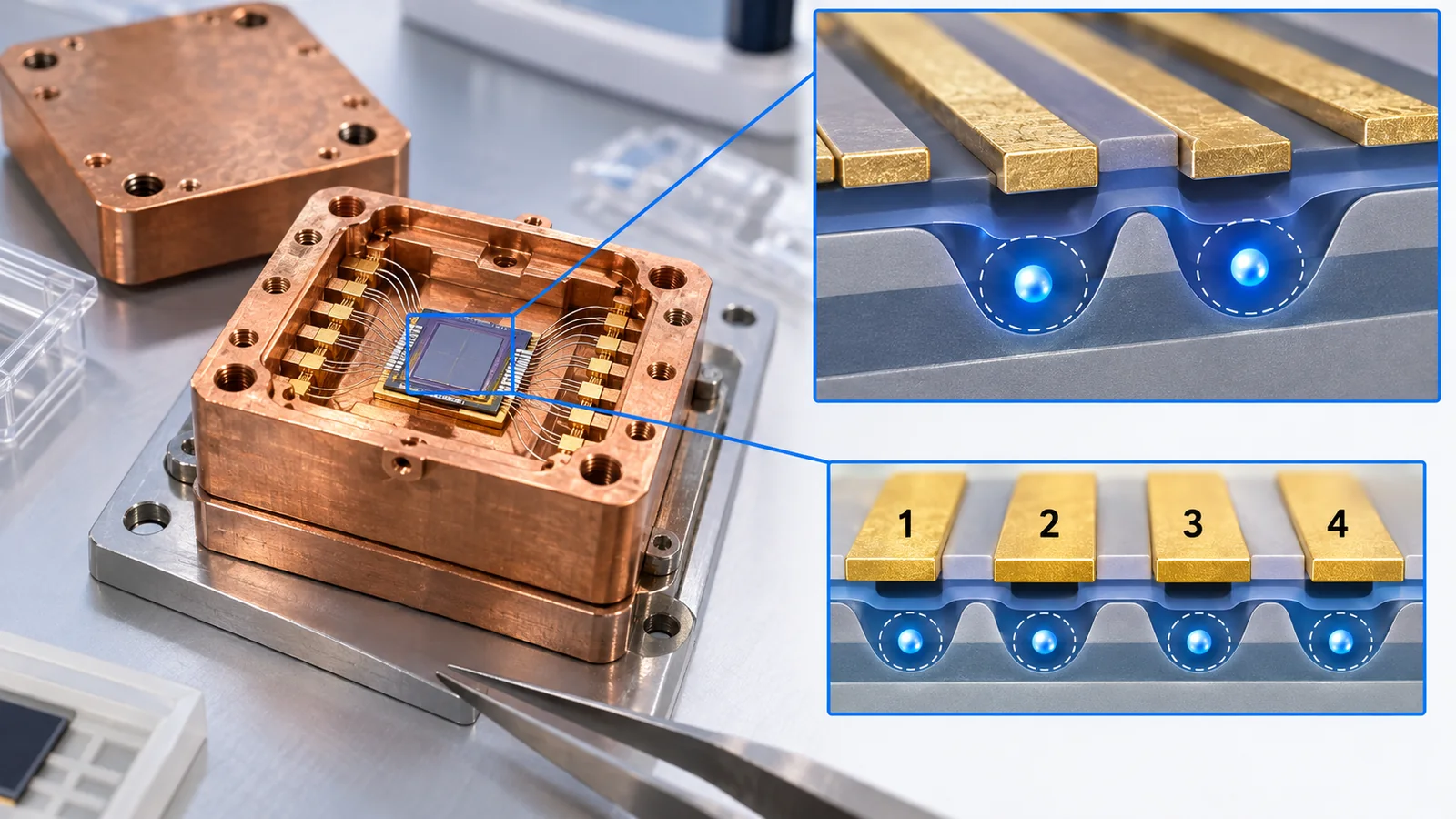
- What it does: a tiny room (a quantum dot) on a semiconductor chip holds exactly one electron, and that electron's spin (the direction of its tiny magnet) is the qubit
- Conclusion: how long an electron spin lasts depends strongly on the nuclear spins of the surrounding atoms. Silicon made only of 28Si, which has no nuclear spin, is therefore an ideal “quiet container.” That is why isotope-purified 28Si is needed
- The most important point: “it can be made in a chip factory” is not the same as “many qubits work together.” In 2025, two-qubit devices made on a 300 mm production line showed fidelities above 99%, but the largest number of qubits reported so far is still a handful, up to eight (checked 16 October 2026)
It helps to know that a qubit can be drawn as an arrow from the centre of a sphere to its surface (north pole = 0, south pole = 1, a tilted arrow = a superposition), and that measuring it gives either 0 or 1. If that is new to you, Chapter 1 explains it briefly. No physics or semiconductor background is needed.
Where this fits in the seriesRead this after our explainers on quantum computing fundamentals, quantum gates and circuits, and coherence and fidelity (the article is still readable on its own, because the needed background is restated briefly). The materials for confining electrons in small rooms are covered in our explainer on quantum dots, magnetic properties in our explainer on spintronic materials, thin-film deposition in our explainer on atomic layer deposition, and inspection techniques in our explainer on nanoscale metrology. Cryogenic equipment is covered in our explainer on cryogenics and control, and the overall materials and fabrication picture in our explainer on materials and fabrication for quantum computers.
- What electron spin is — a tiny magnet's direction
- Magnetic field, energy and temperature — why extreme cold is needed (our calculation)
- Trapping exactly one electron — two ways to build a quantum dot
- Control and readout — rotate with microwaves, read by turning spin into charge
- Why silicon, and why 28Si — the nuisance of nuclear spins
- Interfaces and valleys — material uniformity becomes qubit performance
- Building in a chip factory — where 300 mm wafers stand, and the open problems
- Reading the results — how to take a fidelity number
- Running at higher temperatures, and a summary of strengths and weaknesses
- What we could not confirm, and a summary
- How to read evaluations and standards
- Glossary
- References (primary sources)
- Claim-to-source audit
Sourced = stated in a published source (with a link)
Our calculation = a value this article computed from stated assumptions
Not yet confirmed = plans, targets or drafts that are not settled
Our reading of what this means for materials is marked as commentary. Inference is shown in bold. Company announcements are treated as “company claims” and do not imply independent confirmation.
The numbers in Chapters 2 and 5 are our calculations using physical constants from NIST. The quantum-dot size used there (20 nm × 20 nm × 5 nm) is a made-up example chosen to make the arithmetic easy to follow, not the size of any real device. The fidelities in Chapter 8 were measured with different methods, at different temperatures, on different devices, so that table is not a ranking. A laboratory best value does not describe a production device.
1. What electron spin is — a tiny magnet's direction
First, an everyday picture
Think of a compass needle. The needle is a small magnet that points north or south. An electron has a similar property: it behaves like a tiny magnet that points “up” or “down.” This property is called spin.
Why does this make a qubit? A qubit needs two states that stand for 0 and 1. When a magnetic field is applied, an electron spin separates cleanly into two states: along the field and against it. Assign 0 and 1 to these two, and you have a qubit.
The name suggests that the electron spins like a top, but that picture is not strictly correct. Spin is a quantum-mechanical property of the electron, and it is easier to think about as “the direction of a tiny magnet” when we consider how a qubit works. The picture holds only as far as “the direction can take two values.” A tilted direction (a superposition) is something a real compass needle does not have; it is purely quantum.
Matching it to the qubit arrow
In this series a qubit state is drawn as an arrow from the centre of a sphere to its surface. Pointing at the north pole means 0, at the south pole means 1, and anywhere in between is a superposition of 0 and 1. For an electron spin, you can lay this arrow directly on “the direction of the electron's tiny magnet.” When the arrow is tilted, a measurement gives 0 or 1, and the probability depends on the tilt. After the measurement, the original arrow is not recovered.
Wrong: “because of superposition, it gives the answers for 0 and 1 at once.” In fact: even when the arrow is tilted, a measurement gives either 0 or 1. The strength of a quantum computer comes from adding the arrows of many qubits together like waves (interference), designing the circuit so that correct answers reinforce each other and wrong answers cancel. An electron spin is just one kind of “vessel” that carries such an arrow (see our explainer on quantum computing fundamentals).
Why is electron spin a good qubit candidate?
The review by Burkard and colleagues describes spin as a natural two-level system that is insensitive to electric fields, and says this is why long coherence (the time a quantum state survives) can be obtained Sourced [Ref. 3]. Chips are full of electrical jitter (fluctuating electric fields). Spin is a magnet direction, so it is less sensitive to such electrical jitter. But “less sensitive” does not mean not sensitive. As we will see, the real limits of today's qubits are set by electrical jitter (charge noise) and by nearby nuclear spins.
History in one line
The idea of confining an electron in a quantum dot and using its spin as a qubit was proposed by Loss and DiVincenzo in 1998 Sourced [Ref. 1]. In the same year, Kane proposed a quantum computer that uses the spin of the nucleus of phosphorus atoms in silicon Sourced [Ref. 2]. This article deals mainly with the former (electron spin) and touches the latter (phosphorus atoms, or “donors”) briefly.
2. Magnetic field, energy and temperature — why extreme cold is needed (our calculation)
In a magnetic field, the energy of an electron spin splits in two (Fig. 2). The gap ΔE is the “energy difference between 0 and 1” of the qubit. Here we check how big it is with real numbers.
Step 1: express the energy gap as a frequency
For a free electron spin the frequency per tesla (T) of magnetic field is about 28.02 GHz. The NIST table of physical constants gives the electron gyromagnetic ratio divided by 2π as 28 024.951 MHz/T Sourced [Ref. 4]. For an electron in silicon, the value can shift a little because of valley and interface effects (the review by Burkard and colleagues mentions corrections from the mixing of valley states [Ref. 3]). For example, in the device of Steinacker and colleagues (arXiv version) the field is 0.666 T, the Zeeman energy is about 77 µeV, and the microwave (local oscillator) frequency is 18.610 GHz Sourced [Ref. 19]. Using the free-electron value, 28.025 GHz/T × 0.666 T = about 18.7 GHz, which matches the paper closely Our calculation. A frequency in the 18 GHz range is far above that of a microwave oven (about 2.45 GHz).
Step 2: convert that to temperature
The energy of a frequency f is h × f (h is Planck's constant). Converted this way, ΔE at 0.666 T is about 77 µeV (micro-electronvolts), which corresponds to a temperature of about 0.90 K (kelvin) Our calculation (Planck's and Boltzmann's constants from NIST [Ref. 4]). In other words, at about 0.9 K (−272 °C), the energy of the surrounding thermal jitter is about the same as the up-down energy gap of the spin.
Step 3: heat scrambles the directions
When the thermal jitter is large, spins scatter randomly between up and down. The degree to which they favor the lower-energy direction (the polarization P) can be computed, with thermal energy kBT, as P = tanh(ΔE / 2kBT) (our explanation; this is the standard formula for a two-level system in thermal equilibrium). It means: the larger ΔE is compared with the thermal energy, the closer P gets to 1 (almost all spins in the lower direction). Let us look at numbers.
| Temperature | Thermal energy kBT | P at 0.1 T (ΔE about 11.6 µeV) | P at 0.666 T (ΔE about 77 µeV) | P at 1 T (ΔE about 116 µeV) |
|---|---|---|---|---|
| 10 mK | about 0.86 µeV | about 1.000 | about 1.000 | about 1.000 |
| 100 mK | about 8.6 µeV | about 0.59 | about 0.9997 | about 0.999997 |
| 1 K | about 86 µeV | about 0.07 | about 0.42 | about 0.59 |
| 4 K | about 345 µeV | about 0.02 | about 0.11 | about 0.17 |
Calculation: ΔE = h × 28.025 GHz/T × B, P = tanh(ΔE / 2kBT) (Our calculation). Constants from the NIST physical constants table; the free-electron value is used (it can shift slightly in silicon).
Not necessarily. Low polarization means “you cannot always start the qubit from the same direction (say, 0).” In real experiments, the direction is set at the start by an initialization step, and the starting state can be checked by a measurement, which makes up for it to some degree (our explanation). Still, the calculation shows that lower temperatures make initialization and readout easier to do accurately. Chapter 9 describes work that ran above 1 K.
The main message of this calculation is that temperature is a contest against thermal jitter. Inside the refrigerator the chip is cooled to temperatures such as 10 mK (0.01 K), and the cooling power there is tiny (the paper by Yang and colleagues says the cooling power of dilution refrigerators is extremely limited below 100 mK [Ref. 24]). So the wiring, solder, substrate and adhesives near the chip are chosen to not crack in the cold, not store heat, and not contain magnetic impurities. For a materials engineer, the properties that matter here are not room-temperature ones but thermal conductivity, specific heat and magnetism between a few mK and 1 K (our commentary; cryogenic materials are covered in our explainers on cryogenics and control and on materials and fabrication for quantum computers).
3. Trapping exactly one electron — two ways to build a quantum dot
An everyday picture: put exactly one marble in a small dent
To use an electron spin as a qubit, you have to place exactly one electron at a chosen spot. Imagine pressing a small dent into a flat board and dropping in a single marble. On a semiconductor chip, the dent is made with “voltage.” Thin metal electrodes (gates) are laid on the surface, and applying voltages pulls electrons together or pushes them away just beneath each gate. A small region that traps electrons this way is called a quantum dot (the materials side of quantum dots is covered in our explainer on quantum dots; here the word simply means “a small room that holds one electron at a time”).
The review by Burkard and colleagues also treats the gate-defined quantum dot, in which gate voltages confine the electron, as the basic form of the electron-spin qubit Sourced [Ref. 3].
Two main ways to build it
Silicon quantum dots fall into two main types according to where the electron is held. In a MOS-type dot, the electron sits at the boundary (interface) between silicon and its oxide (SiO2). In a Si/SiGe-type dot, layers of silicon and silicon-germanium alloy (SiGe) are stacked, and the electron sits in a thin silicon layer (a quantum well).
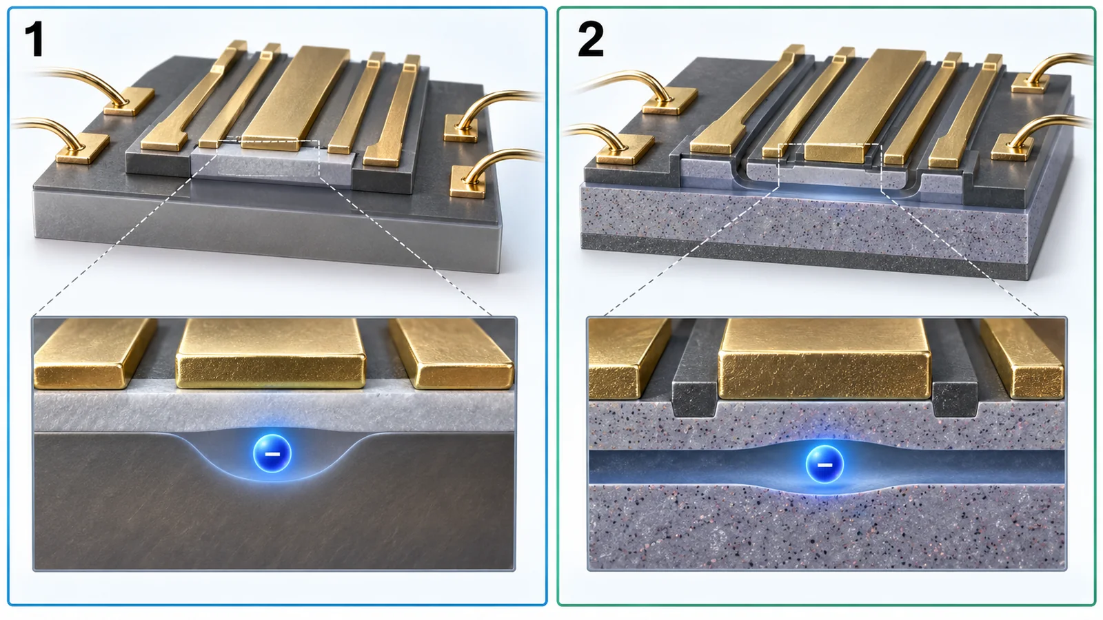
View original SVG, values and sources
Original SVG reference: Conceptual diagram (vector drawing). Cross sections of a MOS-type dot (left) and a Si/SiGe-type dot (right). Layer thicknesses and the number and shape of the electrodes are illustrative, not dimensions of any real device. As an example of the MOS type, the device of Steinacker and colleagues uses a thermal oxide and polysilicon gates [Ref. 19]. As an example of the Si/SiGe type, the device of Noiri and colleagues uses Al gates and a Ti/Co micromagnet [Ref. 13].
| Type | Where the electron sits | What mainly sets the valley splitting (Chapter 6) | Examples (materials and structure as described) |
|---|---|---|---|
| MOS type | The interface between silicon and an oxide (SiO2) | Tunable with a vertical electric field. Reported values range from 50 to 500 µeV [Ref. 3] Sourced | Steinacker et al. (2025): an epitaxially grown 28Si layer, a thermal oxide and three layers of polysilicon gates (as described in the arXiv version) [Ref. 19] Sourced |
| Si/SiGe type | A thin, strained silicon layer (quantum well) sandwiched by SiGe | Weak tuning by electric field; set mainly by interface quality and well width. Up to about 200 to 300 µeV reported for high-quality interfaces and narrow wells [Ref. 3] Sourced | Noiri et al. (2022): a 28Si quantum well 50 nm below the surface, with Al gates and a Ti/Co micromagnet [Ref. 13]. Yoneda et al. (2018): grown by gas-source molecular beam epitaxy [Ref. 12] Sourced |
| Donor type (for reference) | The electron or the nucleus of a phosphorus atom (donor) implanted in silicon | For a donor, the six valleys mix into one state (review by Burkard and colleagues) [Ref. 3] | Muhonen et al. (2014) and Mądzik et al. (2022): devices on a 28Si substrate [Refs. 7, 18] Sourced |
The table is our own organization (Our calculation). Numbers are as stated in each paper or review. It does not argue which type is better.
This “gate” is a different thing from a “quantum gate” in a logic circuit. A quantum gate is an operation; the gate electrode here is a metal plate used to apply a voltage (the same word as the gate of a transistor). Because the two are easy to confuse, this article writes “gate electrode” for the metal plate and “quantum gate” for the operation.
4. Control and readout — rotate with microwaves, read by turning spin into charge
To use an electron spin as a qubit you need three things: prepare it, rotate it, and read it. Each is explained below with methods used in actual experiments.
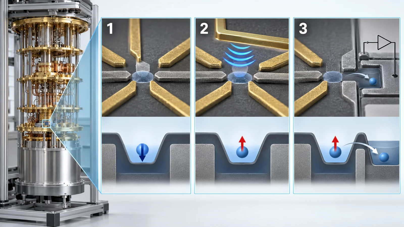
View original SVG, values and sources
Original SVG reference: Conceptual diagram (vector drawing). The basic flow of an electron-spin qubit. In real experiments, preparation, control and readout are repeated many times, and quantities such as fidelity are obtained from the fractions of outcomes. Symbols and layout in the figure are illustrative.
1. Prepare — align the direction and start
First, the qubit is prepared in state 0. In silicon spin qubits, the device is cooled so that the electron tends to point in the lower-energy direction (the calculation in Chapter 2). In the experiment of Steinacker and colleagues, the quantum dots were disconnected from the electron reservoir and loaded with four electrons (as described in the arXiv version) [Ref. 19].
2. Control — rotate the arrow with microwaves
When a microwave magnetic field at the frequency that matches the up-down energy gap ΔE is applied, the arrow rotates (the principle of magnetic resonance; Fig. 2 in Chapter 1). The length of the pulse sets the rotation angle. This is a single-qubit gate.
There are two ways to deliver the microwaves, depending on the experiment. Steinacker and colleagues drive a current through an aluminium line (a stripline) near the device to make the microwave magnetic field Sourced [Ref. 19]. Noiri and colleagues use the gradient of the magnetic field made by a small magnet (a Ti/Co micromagnet) on top of the device, and rotate the spin by shaking the electron very slightly with gate voltages Sourced [Ref. 13]. The latter has the advantage that the spin can be driven with electrical signals alone.
For a two-qubit gate, the barrier between two neighboring electrons is lowered with the voltage on a gate electrode (J in Fig. 4). The two electrons then interact slightly (the exchange interaction), so that the direction of one spin affects the other. Petit and colleagues reported that the strength of this coupling could be tuned with gate voltage from 0.5 to 18 MHz Sourced [Ref. 23].
3. Read out — turn the spin direction into presence or absence of charge
The direction of a spin is hard to measure directly. So the spin direction is first turned into the presence or absence of charge, and that is measured. In 2004, Elzerman and colleagues read out the spin direction of a single electron in a quantum dot electrically in a single measurement (spin-to-charge conversion, with detection by a nearby charge detector) Sourced [Ref. 27]. In today's silicon devices, a method based on the Pauli spin blockade is used: whether an electron can hop to the neighboring dot depends on whether two spins point the same way or differently. The review by Burkard and colleagues explains that this maps the spin state onto the charge configuration Sourced [Ref. 3]. The difference in charge configuration is detected as a change in current by a nearby charge sensor (such as a single-electron transistor) [Ref. 19].
Electrons obey a rule: two electrons in the same state cannot occupy the same place (the Pauli exclusion principle). If two electron spins point in opposite directions, one can hop into the neighboring dot and sit in the same place. If they point the same way, it cannot, and it stays put. This difference turns “whether the two spins are the same or different” into how easily charge moves (our explanation). This method reads a property of a pair, not a single spin, so the readout design becomes a little more involved.
The device of Noiri and colleagues has aluminium gates (with a thin native oxide on the surface), on top of that an alumina insulating film (30 nm) made by atomic layer deposition (ALD), and on top of that a Ti/Co micromagnet Sourced [Ref. 13]. In other words, the composition and thickness of the magnetic film and the quality of the insulating film are tied to how fast the qubit can be controlled and how large the surrounding noise is. Variation in the field made by the magnet material and the charge jitter inside the insulator are materials problems (our commentary; ALD is covered in our explainer on atomic layer deposition, magnetic materials in our explainer on spintronic materials).
5. Why silicon, and why 28Si — the nuisance of nuclear spins
The question: what disturbs an electron spin?
Electron spins were insensitive to electrical jitter. So what does damage a qubit? One major cause is the nuclei of the surrounding atoms. Some atomic nuclei have a tiny-magnet property of their own (nuclear spin). When many such nuclear magnets sit near an electron, the electron feels the faint magnetic field they produce. That field fluctuates as the nuclear magnets slowly change direction, and the electron spin's arrow gradually blurs.
The review by Burkard and colleagues says that in GaAs (gallium arsenide) quantum dots, the fluctuating nuclear field limits the dephasing time T2* to about 10 ns Sourced [Ref. 3]. In GaAs every atom has a magnetic nucleus. Silicon is different.
Silicon isotopes — some carry a magnet, some do not
Even within one element, there are varieties with different nuclear masses, called isotopes. Natural silicon contains 92.223% 28Si, 4.685% 29Si and 3.092% 30Si (NIST) Sourced [Ref. 5]. Of these, only 29Si has a nuclear spin (a magnet property); 28Si and 30Si do not (our explanation; Tyryshkin and colleagues describe 28Si as a form of silicon with no magnetic nuclei [Ref. 6]). So silicon made only of 28Si is a “quiet container” with no disturbing magnets around.
Picture the electron spin as a person speaking quietly in a classroom. Natural silicon is a classroom where about one child in twenty is chatty (29Si). The voices of nearby children fluctuate and the conversation gets blurred. The 28Si classroom has almost no chatty children.
Limits of the analogy: the nuclear spins of 29Si do not jump around randomly and quickly; they change direction slowly, so the noise is “slow noise.” That is why a spin echo (an operation that cancels it later) can remove much of it (our explanation).
How quiet does it get? — numbers from experiments
Using 28Si greatly extends how long spin coherence lasts. Here are some results using donors (phosphorus atoms).
- Tyryshkin et al. (2012): in high-purity 28Si with less than 50 ppm residual 29Si, the coherence time T2 of donor electron spins reached up to 2 seconds. Suppressing interactions between electrons gave an extrapolated 10 seconds at 1.8 K Sourced [Ref. 6]. (ppm means parts per million. This was a measurement on an ensemble of many spins.)
- Muhonen et al. (2014): in a gated device on a 28Si substrate, the coherence of the nuclear spin of a single phosphorus atom exceeded 30 seconds (using a pulse sequence called CPMG), with control fidelity above 99.99%. The CPMG coherence time of the electron spin exceeded 0.5 seconds Sourced [Ref. 7].
For the electron spin in a quantum dot, on the other hand, Yoneda and colleagues (2018) reported, in a 28Si/SiGe device, a dephasing time (T2*) of 20 µs, an average single-qubit gate fidelity above 99.9%, and charge noise as the main cause of the fluctuations Sourced [Ref. 12]. Note that the quantum-dot electron (tens of µs) is far shorter than the donor nuclear spin (seconds). This is because a quantum-dot electron is easy to drive electrically but is therefore also sensitive to electrical jitter (charge noise) (our explanation).
How many 29Si atoms remain? (our calculation)
“800 ppm of 29Si remains” is hard to feel, so let us convert it to a count. The lattice constant of the silicon crystal is 0.5431 nm (NIST), and one cubic unit cell holds 8 atoms. So the number of silicon atoms per cm3 is 8 / (0.5431 nm)3 = about 5.0 × 10²² Our calculation [Ref. 4].
Suppose the electron occupies a region of 20 nm × 20 nm × 5 nm (a made-up size for explanation, not the size of any real device). That volume is 2.0 × 10⁻¹⁸ cm3 and holds about 100,000 silicon atoms. The number of 29Si among them is about 4,700 in natural silicon, about 80 at 800 ppm, about 40 at 400 ppm, and about 5 at 50 ppm Our calculation.
A count must be a whole number, so “average 0.08” means if you look at 100 regions of the same size, about 8 of them contain a 29Si atom. Most quantum dots end up completely “quiet,” with no 29Si at all. Natural silicon, by contrast, puts thousands of nuclear spins around every quantum dot, and fluctuations in their directions ride on the electron spin.
How is 28Si made?
Isotopes behave almost identically in chemistry, so ordinary chemical purification cannot separate them (our explanation). They are separated by their difference in mass instead.
- Industrial methods such as gas centrifuges: Dwyer and colleagues called this approach “industrial gas centrifuges” and studied an alternative [Ref. 8].
- Mass selection of ions: Dwyer et al. (2014) made silicon ions from commercial silane (SiH4), sorted them by mass in a magnetic field and deposited them on a Si(100) substrate, obtaining films in which the fractions of both 29Si and 30Si are below 1 × 10⁻⁶ Sourced [Ref. 8]. Tang et al. (2020) used a similar ion-beam deposition to grow 28Si films with controlled enrichment from the natural ratio up to 99.99987% (0.832 × 10⁻⁶ of 29Si) Sourced [Ref. 9]. Both are laboratory-scale.
- Growth from purified silane: Yoneda and colleagues grew a strained 28Si well by gas-source molecular beam epitaxy from isotope-purified silane (about 800 ppm of 29Si) [Ref. 12]. Mazzocchi and colleagues report a CVD-grown 28Si epitaxial film (99.992%) on 300 mm substrates (as given in the title) Sourced [Ref. 10].
An overview of isotope-controlled materials (silicon and diamond) is given in the review by Itoh and Watanabe [Ref. 11].
No. Takeda and colleagues (2016) showed a spin qubit with fault-tolerant control addressing in a quantum dot made of silicon with the natural isotope ratio (as given in the title) Sourced [Ref. 41]. Still, removing the fluctuations from residual 29Si makes higher performance easier to reach, as described above. Steinacker and colleagues, using a device with 400 ppm of 29Si, reported that the main operational errors came from residual nuclear-spin isotopes and not from charge noise, and they say purification to 50 ppm or below could improve this Sourced [Refs. 19, 20]. That, however, is the authors' outlook and not a demonstrated result Not yet confirmed.
In semiconductor materials, impurity concentration (ppm to ppb) is the usual thing to control. For 28Si, the isotope ratio (how many ppm of 29Si remain) is a second metric that links directly to device performance. Even with perfect chemical purity, a high 29Si content will hold performance back. Conversely, a good isotope ratio does not help if oxygen, carbon or metal impurities act as another noise source (our commentary).
Also, the region where the electron lives is only a few tens of nm of the well (in the device of Noiri and colleagues the quantum well is 50 nm below the surface [Ref. 13]). This is an inference, but “purifying only the layer where the electron lives” might cut the amount of 28Si feedstock required. In fact, Yoneda and colleagues state that they used purified silane only for growing the strained well [Ref. 12]. We could not confirm the supply volume or price of the feedstock.
6. Interfaces and valleys — material uniformity becomes qubit performance
Charge noise — the other wall
Even after nuclear spins are removed with 28Si, another wall remains: charge noise. An electron spin is insensitive to electric fields, but in a quantum dot the spin is driven with the help of electric fields. As a result, it also picks up the jitter of the electric field (charge noise). Yoneda and colleagues showed that the dephasing was caused not by magnetic noise but by charge noise (of the 1/f type, whose power is inversely proportional to frequency), and that this 1/f spectrum extends over seven decades of frequency Sourced [Ref. 12]. In the device of Steinacker and colleagues, charge noise measured with a single-electron transistor was about 0.8 µeV/√Hz at 1 Hz, similar to the low values of earlier similar devices (arXiv version) Sourced [Ref. 19].
The cause of charge noise is thought to be defects and impurities in the oxide and at the interface that capture and release electrons (general understanding; our explanation). This is where materials engineers come in. Interface quality, defects in films and control of metal impurities decide qubit performance.
Valleys — a nuisance unique to silicon
Silicon has one more problem of its own: valleys. An electron in a crystal spreads out as a wave. In silicon there are six different “wave shapes” with the lowest energy (the review by Burkard and colleagues: the conduction-band minimum is six-fold degenerate) Sourced [Ref. 3]. The electron may be in any of these six “valley bottoms,” and these are the six valleys (this concerns the wavelength of the electron's wave, not a real hill or valley).
In a quantum dot, only the two valleys along the confinement direction (vertical) matter. In MOS devices the vertical electric field, and in Si/SiGe devices the strain, lifts the other four valleys. The energy difference between the two remaining valleys is called the valley splitting Sourced [Ref. 3].
What goes wrong if valley splitting is small?
If the valley splitting is close to, or smaller than, the spin's energy gap (the Zeeman energy), the spin state mixes with the valley state and the qubit becomes hard to use (our explanation; the review says that mixing of valley states affects the g-factor and spin relaxation [Ref. 3]). Yoneda and colleagues write that they confirmed by magneto-spectroscopy that the valley splitting was much larger than the Zeeman splitting [Ref. 12]. As the lower half of Fig. 7 shows, against 77 µeV at 0.666 T, the lower end of the reported MOS range (50 µeV) is below it. So the size of the valley splitting has to be checked device by device (our reading).
Si/SiGe devices have another problem. Paquelet Wuetz and colleagues explained that concentration fluctuations of Si and Ge atoms at each three-dimensional spot of the interface make valley splitting vary widely across many devices Sourced [Ref. 28]. Against prevailing belief, they propose adding some Ge to the well to increase these fluctuations and so raise the valley splitting statistically [Ref. 28]. The key point is that a flat and uniform interface translates directly into uniform qubits.
Wrong: “semiconductor technology is mature, so qubits are easy to build.” In fact: an ordinary transistor works fine with millions of electrons moving. A qubit has to keep the direction of one electron almost undisturbed, so single defects, atomic-scale roughness and mixed isotopes that do not matter for transistors decide performance (our explanation). The same name, “silicon,” hides a different kind of quality requirement.
In MOS devices, defects at the Si/SiO2 interface and roughness of the interface decide charge noise and valley splitting. In Si/SiGe devices, how strain enters SiGe, how sharp the interface is and how Ge is distributed decide the spread in valley splitting [Ref. 28]. In both types, process control of epitaxial growth, oxidation and cleaning that is uniform at the atomic-layer level is needed, and reproducibility of manufacturing is an important metric for a production process (our commentary; thin-film and interface characterization is covered in our explainer on nanoscale metrology).
7. Building in a chip factory — where 300 mm wafers stand, and the open problems
Why does “can be made in a factory” matter?
A practical quantum computer is expected to need a very large number of qubits in order to correct errors. Neyens and colleagues state that putting millions of qubits on one processor with solid-state devices will require device fabrication on a scale comparable to the modern CMOS industry Sourced [Ref. 22]. That is why the existing mass-production infrastructure of semiconductor factories is attractive for making qubits, and it is the main motivation behind silicon spin qubits.
But whether a high-performance device made in a research lab can also be made the same way in a factory was a separate question. At the start of their paper, Steinacker and colleagues write that it had not been clear whether the excellent fidelities and long coherence shown by devices made in a lab could be reproduced by devices made in a semiconductor foundry (a contract manufacturing plant) Sourced [Ref. 20].
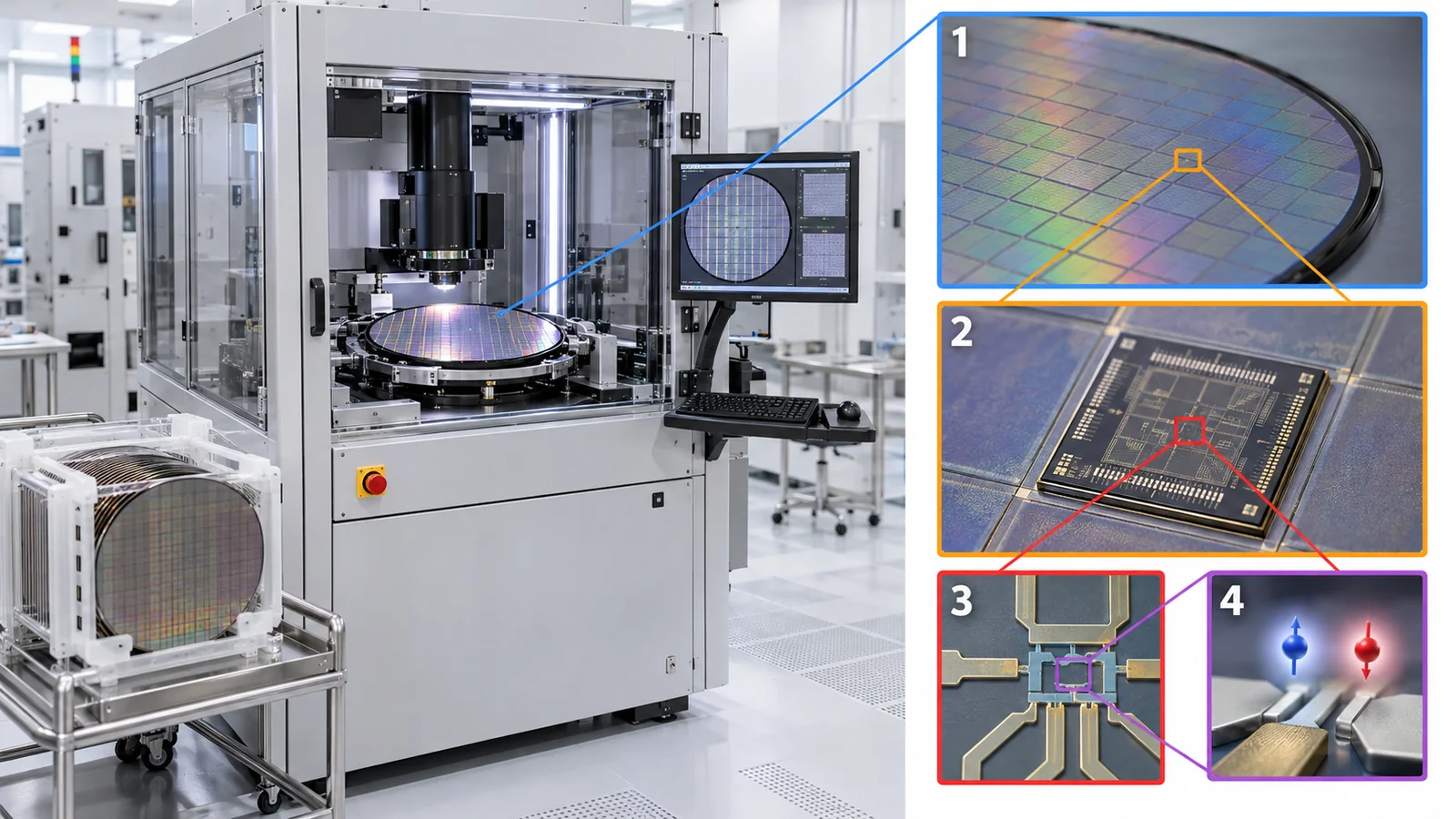
The flow of building in a factory
Steinacker and colleagues write that the device was designed by Diraq and fabricated in a 300 mm spin-qubit process at imec. The gate pitch is below 100 nm, and optical lithography and electron-beam lithography (EBL) are combined to allow fast cycles and design flexibility (arXiv version) Sourced [Ref. 19]. In other words, even in a “300 mm factory,” the finest parts of the qubit include patterns drawn with an electron beam. Intel, by comparison, says it made Tunnel Falls on 300 mm wafers in its most advanced transistor fabrication facility, including extreme ultraviolet (EUV) lithography (company claim) [Ref. 26].
Main results so far (checked 16 October 2026)
| Organization, year | Scale and main numbers | Nature of the information |
|---|---|---|
| Intel: Tunnel Falls (announced 15 June 2023) | A device with 12 quantum dots (usable as 4 to 12 qubits). 300 mm wafers, the company's D1 facility. “95% yield across the wafer” and “voltage uniformity similar to a CMOS logic process” | Company claim (Intel announcement) [Ref. 26] Sourced (that it was announced) |
| Intel: Neyens et al. (Nature, May 2024) | Measured hundreds of devices at 1.6 K with a cryogenic 300 mm wafer prober. Reported small spread in single-electron operating voltages and little disorder at wafer scale | Peer-reviewed paper [Ref. 22] Sourced |
| imec and Diraq: Steinacker et al. (Nature, September 2025) | In four two-qubit devices made in a 300 mm foundry, single- and two-qubit control fidelities all exceed 99%, and state preparation and measurement fidelity reaches up to 99.9% (gate set tomography). T1 = 9.5 s, T2* = 40.6 µs, T2Hahn = 1.9 ms (maximum values) | Peer-reviewed paper [Ref. 20] Sourced |
| Same: “randomly selected devices” | The announcement by imec and Diraq says the results came from randomly selected devices rather than “hero devices” | Company claim (Diraq announcement) [Ref. 42] |
| Diraq, imec and others: Nickl et al. (preprint, December 2025) | Tuned an eight-dot linear array (four pairs). T2* up to 41 µs, T2Hahn up to 1.31 ms. Demonstrated a two-qubit gate between adjacent qubits. Readout of the central four qubits by cascaded charge sensing | Preprint [Ref. 21] Sourced. Press reports say it was published in Nature Communications, but we could not confirm the journal page |
| DARPA: QBI Stage C (announced 7 October 2026) | Four organizations, including Diraq (silicon CMOS spin qubits), were announced as moving from Stage B to the final stage, Stage C. Stage C is where a government evaluation team tests whether proposed utility-scale systems can be built as designed and operated as intended | Public agency announcement [Ref. 44] Sourced. It is not a certification that a utility-scale machine has been achieved (our explanation) |
Numbers are as stated in each paper or announcement. Checked 16 October 2026. We could not find gate-fidelity numbers for the eight-qubit work (none in the abstract). The table is our own organization (Our calculation).
Wrong: “it was made in a factory, so mass production will give millions of qubits.” In fact: the number of qubits reported on factory-made devices, as of 2025 and 2026, ranges from two (four devices) to eight (table above). The purpose of building in a factory is to check that a route exists to making many qubits with the same quality in the future. Figures such as millions of qubits are company targets (Not yet confirmed), not achieved facts. For example, Diraq states plans of thousands of qubits in 2029 and more than one million in 2031 (a company claim, from an article reporting its announcement) [Ref. 43].
Steinacker and colleagues write that in MOS gate stacks, initialization, readout and exchange-based two-qubit gates are sensitive to charge noise, and that this motivated the approach of moving the electron away from the interface into a quantum well. On the other hand, forming quantum dots against thin oxides has benefits, including a large valley splitting from the strong electric field and efficient coupling between gate voltage and channel (arXiv version) Sourced [Ref. 19]. So the choice of materials is a trade-off: what helps one thing hurts another.
Note that Neyens and colleagues use the “spread in single-electron operating voltages” as their metric [Ref. 22]. This is an electrical uniformity at cryogenic temperature that room-temperature dimension measurements cannot see. Through a materials engineer's eyes, the density of defects on the wafer and the distribution of charge in films show up directly as voltage spread (our commentary).
8. Reading the results — how to take a fidelity number
How impressive is “99.5%”?
The fidelity of a quantum gate expresses “how closely the ideal operation was carried out” (see our explainer on coherence and fidelity). At a fidelity of 99.5%, the error is 0.5%, so on average one operation in 200 fails Our calculation. At 99.9% it is one in 1,000, and at 99.99% one in 10,000.
A useful yardstick is the threshold of an error-correcting code. Fowler and colleagues showed that for the surface code, error correction starts to work when the error rate is about 1% or lower Sourced [Ref. 36] (see our explainer on quantum error correction and the surface code). Noiri and colleagues reported that two-qubit gate fidelity of electron-spin qubits had been limited to 98%, and that they now obtained 99.5% (and 99.8% for single-qubit gates) Sourced [Ref. 13].
No. What passed the threshold is the accuracy of individual operations. For error correction to actually work, many qubits must all run at this accuracy together, with good readout and state preparation, and errors must not spread among qubits (our explanation). Takeda and colleagues demonstrated a three-qubit phase-correcting code in silicon, but that is a small code that corrects only one kind of error (phase flips) [Ref. 16]. Practical-scale error correction such as a surface code has not yet been demonstrated with silicon spin qubits (as far as we could confirm).
Number of qubits, and performance achieved at the same time
In 2022, Philips and colleagues built a six-qubit processor in silicon and reported running operations, state preparation and measurement together at respectable fidelities Sourced [Ref. 17]. The authors write that increasing the number of qubits and keeping high fidelity are usually conflicting requirements. As seen above, factory-made devices have been confirmed up to eight qubits (preprint) [Ref. 21].
In other words, the strength of silicon spin qubits lies in the performance of each individual qubit (long coherence and high fidelity) and in the way they are made, while the number of qubits is something still to be increased (our summary; checked 16 October 2026).
In addition, Mills and colleagues of Princeton reported a two-qubit silicon quantum processor with operation fidelity exceeding 99% (as given in the title) Sourced [Ref. 15]. Mądzik and colleagues, using the donor type with the nuclear spins of phosphorus atoms, reported a single-qubit gate fidelity of up to 99.95% and a two-qubit gate fidelity of 99.37% (evaluated with gate set tomography) Sourced [Ref. 18].
9. Running at higher temperatures, and a summary of strengths and weaknesses
Why raise the temperature?
As the calculation in Chapter 2 showed, low temperatures favor running a qubit in a good state. But the cooling power of a refrigerator is smaller the colder it runs. Yang and colleagues point out that for solid-state qubits, each additional qubit adds heat, while the cooling power of dilution refrigerators is extremely limited below 100 mK Sourced [Ref. 24]. So researchers are looking for qubits that work at higher temperatures (above 1 K).
- Petit et al. (2020): reported that silicon quantum dots can execute a universal gate set (single- and two-qubit gates) above 1 K. Single-qubit gate fidelity was up to 99.3%, and the exchange interaction could be tuned from 0.5 to 18 MHz Sourced [Ref. 23].
- Yang et al. (2020): operated a two-qubit unit cell in 28Si at about 1.5 K, with single-qubit gate fidelity of 98.6% and a coherence time of 2 µs, comparable to spin qubits in natural silicon measured at millikelvin temperatures. The field could be lowered to 0.1 T. Initialization and readout used only tunneling of electrons between quantum dots, with the dots isolated from the reservoir Sourced [Ref. 24].
- Camenzind et al. (2022): made a qubit from the spin of a hole (a missing electron) in a silicon FinFET (fin-shaped transistor) and operated it above 4 K, with a drive frequency up to 150 MHz and single-qubit gate fidelity at the fault-tolerance threshold Sourced [Ref. 25].
The polarization calculation in Chapter 2 applies when the spins are aligned by heat alone. Yang and colleagues instead initialize and read out only by letting electrons tunnel between quantum dots [Ref. 24]. So the disadvantage of higher temperature can be avoided to some extent by how the operation is designed (our explanation). Coherence does tend to get shorter at higher temperature, though, and the 2 µs of Yang and colleagues is far shorter than the T2Hahn (up to 1.9 ms) of the factory-made devices in Chapter 7 (the conditions differ, so they cannot be compared directly).
Running at 1 K gives more cooling power, so it becomes easier to place more wiring and heat-generating control circuits near the qubits. Camenzind and colleagues say that raising the operating temperature opens a path to putting quantum hardware and classical control electronics on the same chip [Ref. 25]. Xue and colleagues report an experiment in which a CMOS cryogenic control circuit controlled a silicon quantum circuit (as given in the title) Sourced [Ref. 30]. From the materials side, the low-temperature behavior (mobility, threshold voltage, noise) of transistors, wiring metals and insulating films that keep working in the cold becomes a new set of evaluation items (our commentary; cryogenic control is covered in our explainer on cryogenics and control).
Strengths and weaknesses (no ranking against other platforms)
| Aspect | Strengths that can be confirmed | Challenges that can be confirmed |
|---|---|---|
| Manufacturing | Two-qubit devices with fidelity above 99% made in a 300 mm factory (Steinacker et al.). Cryogenic testing of hundreds of devices on a wafer (Neyens et al.) [Refs. 20, 22] Sourced | An electron-beam step is used for the finest structures in some cases [Ref. 19]. The largest reported qubit count is about eight (preprint) [Ref. 21] Sourced |
| Coherence and fidelity | T1 of seconds and T2Hahn of milliseconds. Single-qubit fidelity above 99.9% and two-qubit fidelity of 99.5% (Noiri, Xue) [Refs. 12, 13, 14, 20] Sourced | Charge noise and residual 29Si nuclear spins are reported as the main sources of error [Refs. 12, 19] Sourced |
| Materials | With 28Si, the main noise source, nuclear spins, can in principle be removed [Refs. 6, 7] Sourced | Isotope purification, valley splitting and interface uniformity are open issues. Valley splitting varies from device to device [Refs. 3, 28] Sourced |
| Operating temperature | Operation reported above 1 K and even above 4 K (with different devices and conditions) [Refs. 23, 24, 25] Sourced | Coherence tends to get shorter at higher temperature (the 2 µs of Yang et al.) [Ref. 24] Sourced |
| Scaling up | A path to putting control circuits on the same chip (Camenzind et al.). As an example of two-dimensional dot arrays, four qubits with germanium hole spins (Hendrickx et al.) [Refs. 25, 29] Sourced | The two-qubit gate was demonstrated between adjacent qubits (Nickl et al.). How to handle many qubits with wiring, readout and calibration is still being researched [Ref. 21] Sourced |
The table is our own organization (Our calculation). It is not a judgment of which is better. For comparison with other platforms (superconducting, ion, neutral atom, photonic), see the explainer for each platform in this series. Devices differ in conditions from paper to paper.
10. What we could not confirm, and a summary
What we could not confirm
- The full text of the Nature version of Steinacker et al.: we checked the abstract, but details such as the residual 29Si level (400 ppm) were checked in the arXiv version (October 2024, second version). The numbers in the Nature full text may differ (the Nature version has four devices and the arXiv version one, and values such as T2* also differ).
- The journal for the eight-qubit paper: we checked the preprint, but could not confirm publication in Nature Communications (as press reports say) on a journal page. The abstract does not give gate-fidelity numbers.
- Intel's situation from 2024 onward: we have not checked the current state of Intel's silicon spin-qubit work after Tunnel Falls (2023) and Neyens et al. (2024).
- Secondary reports that logical operations were demonstrated with silicon spin qubits in 2026: we saw them, but could not confirm the primary paper, so we do not include them.
- Supply volume and price of 28Si feedstock, and the purity each company uses: not confirmed.
- Standards specific to silicon spin qubits: not confirmed (Chapter 11).
- Materials other than silicon, such as germanium hole spins: only touched on.
- An electron spin is the direction of a tiny magnet, and a magnetic field splits it into two. These two are used as 0 and 1. At 0.666 T that is about 18.7 GHz and about 77 µeV (equivalent to about 0.9 K) Our calculation
- Temperature is a contest against thermal jitter. At 1 K the polarization falls to about 0.42 (for 0.666 T), so colder is better. Even so, there are reports of operation above 1 K thanks to clever operation design Sourced / Our calculation
- 28Si is a “quiet container.” Natural silicon has 4.685% 29Si (about 4,700 atoms in a region of about 100,000 atoms). Experiments use 400 to 800 ppm (about 40 to 80 atoms), and laboratories have reached under about 1 ppm Sourced / Our calculation
- The materials problem is at the interface. Charge noise and valley splitting are set by defects, roughness and compositional variation in the oxide or SiGe Sourced
- Two-qubit devices made in a 300 mm factory exceeded 99% (2025). But the qubit count is still at most eight (preprint), and scaling up and demonstrating error correction are still ahead Sourced / Not yet confirmed
11. How to read evaluations and standards
The progress of silicon spin qubits is measured with several “yardsticks”: fidelity (how correct operations are), coherence time (how long the state is kept), accuracy of readout and state preparation, number of qubits, and uniformity of manufacturing. No single one tells the whole story. The number of qubits alone does not show performance, and a fidelity can mean different things depending on how it was measured (randomized benchmarking or gate set tomography) and on temperature and conditions. On the standards side, terminology standards are taking shape, but we could not confirm any evaluation standard specific to silicon spin qubits (checked 16 October 2026).
| What is evaluated | Representative benchmark or method (name, source) | Standards and guidance (ISO/IEC, IEEE and others) | Cautions in reading |
|---|---|---|---|
| Gate fidelity | Randomized benchmarking (Knill et al., 2008; Magesan et al., 2011) [33, 34]. Gate set tomography (Nielsen et al., 2021) [35] Sourced | Not confirmed | RB measures the average error. GST can break errors down by type (stochastic or coherent). Check which method gave the value |
| Threshold guide | The surface-code threshold is about 1% (Fowler et al., 2012) [36] Sourced | Not confirmed | The threshold depends on the code and the noise assumptions. “Exceeded” does not mean error correction works (Chapter 8) |
| Coherence times (T1, T2*, T2Hahn) | Measurement procedures in each paper (Ramsey, Hahn echo, CPMG and others) [12, 19, 20] Sourced | Not confirmed | T2*, T2Hahn and CPMG use different pulse sequences and give very different values (for example 40.6 µs and 1.9 ms). Do not rank devices of different platforms by these values |
| Manufacturing uniformity and yield | Measuring hundreds of devices with a cryogenic wafer prober (Neyens et al., 2024) [22] Sourced | Not confirmed. ISO/IEC JTC 3 excludes some fields, including semiconductors, from its scope [39] Sourced | For yield figures (company claims), check whether the definition of a good device is given [26] |
| Terminology | — (a terminology standard, not an evaluation) | ISO/IEC 4879:2024 “Information technology — Quantum computing — Vocabulary” (published May 2024, first edition) [38] Sourced. IEEE P7130 “Standard for Quantum Technologies Definitions” (draft; PAR approved 23 September 2021, status “Active PAR”) [40] Not yet confirmed | We did not check the text of the standards and do not describe the definitions. On the official JTC 3 page, one standard is published and twelve are under development (as displayed on the check date) [39] |
| Framework of physical requirements | DiVincenzo's five plus two criteria (2000) [37] Sourced | Not confirmed | A framework for checking each platform on qubit definition, initialization, long coherence, universal gates and measurement |
| Benchmark standards (IEEE P7131 and others) | Not confirmed | Not confirmed (we could not retrieve the official page) | Standardization of quantum computer performance evaluation is reported to be in progress, but we did not check its status |
The table is our own organization (Our calculation). Numbers in brackets are reference numbers. ISO and IEEE numbers, titles and status were checked on the official pages (16 October 2026). Standards texts are paywalled, so we limit ourselves to titles and scope.
Cautions in reading (for materials engineers)
- “How many qubits” alone does not show performance: for silicon spin qubits, which have two to eight qubits, fidelity and coherence numbers are ahead of qubit count. Comparing them naively with platforms that have more qubits is meaningless. Always check whether qubits are physical or logical (all numbers in this article are physical qubits)
- A laboratory best value and a factory “uniform value” are different things: Yoneda et al. (single-qubit above 99.9%) and Steinacker et al. (above 99% on all four devices) are both important, but they mean different things. The latter shows reproducibility (whether devices come out alike)
- A company announcement and independent verification are different: Intel's 95% yield, Diraq's random selection and future qubit targets are company claims. Read them apart from what peer-reviewed papers confirm
- Standards are mostly recommendations, not requirements: ISO/IEC 4879 is a terminology standard and does not decide pass or fail on performance (our explanation). Treat plans and targets (qubit counts, years) as Not yet confirmed, not as achieved facts
12. Glossary
- Qubit
- The unit of information in a quantum computer, with two states (0 and 1). In this series it is drawn as an arrow on a sphere.
- Spin
- The tiny-magnet property of an electron and similar particles. The direction takes two values. Nothing is literally rotating.
- Zeeman splitting
- The splitting of the up and down spin energies in a magnetic field. The gap is proportional to the field.
- Polarization
- How strongly spins favor the lower-energy direction. It falls as temperature rises.
- Quantum dot
- A small region that traps electrons, like an artificial atom. Here, a small room that holds one electron.
- Gate electrode
- A metal plate whose voltage gathers or pushes away electrons. Not the same as a quantum gate (an operation).
- MOS type
- A quantum dot that holds the electron at the interface between silicon and its oxide.
- Si/SiGe type
- A quantum dot that holds the electron in a thin silicon layer sandwiched by SiGe.
- Isotope
- A variety of one element with a different nuclear mass. Chemically almost identical.
- 28Si / 29Si
- 28Si is the isotope without nuclear spin; 29Si is the one with nuclear spin.
- ppm
- Parts per million. 1 ppm is one in a million.
- Nuclear spin
- The tiny-magnet property of an atomic nucleus. A noise source for electron spins.
- ESR / EDSR
- Rotating a spin with a microwave magnetic field (ESR). Rotating it with electric fields and a micromagnet (EDSR).
- Exchange interaction
- The coupling between two neighboring electrons. Used for two-qubit gates.
- Pauli spin blockade
- When two spins point the same way, an electron cannot hop to the neighboring dot. Used for readout.
- Single-electron transistor (SET)
- A charge sensor that detects one electron coming and going as a change in current.
- Valley / valley splitting
- The six ways an electron's wave can fit silicon. In a dot, the energy difference between the two remaining valleys is the valley splitting.
- Charge noise / 1/f noise
- Fluctuating electric fields caused by nearby defects capturing and releasing electrons. Stronger at lower frequencies.
- T1 / T2 / T2*
- The time for a spin to relax back (T1) and the time its phase stays aligned (T2, T2*). The value depends on how it is measured.
- Hahn echo
- Flipping the spin midway to cancel slow noise. T2Hahn is the resulting time.
- Fidelity
- How close an actual operation is to the ideal one. At 99.5%, the error is 0.5%.
- Gate set tomography (GST)
- Characterizing a whole set of gates in detail, including the type of each error.
- Randomized benchmarking (RB)
- Repeating random gate sequences to measure the average error.
- Donor
- An atom such as phosphorus placed in silicon. Its spare electron or nuclear spin can be a qubit.
- Dilution refrigerator
- A machine that cools to a few mK. Its cooling power is small.
- Foundry
- A contract factory that makes chips designed by other companies.
- Threshold (error correction)
- The error level below which error correction can improve performance. About 1% for the surface code.
13. References (primary sources)
- Loss D., DiVincenzo D. P. "Quantum computation with quantum dots", Phys. Rev. A 57, 120–126 (1998), DOI 10.1103/PhysRevA.57.120 — doi.org/10.1103/PhysRevA.57.120
- Kane B. E. "A silicon-based nuclear spin quantum computer", Nature 393, 133–137 (1998), DOI 10.1038/30156 — doi.org/10.1038/30156
- Burkard G., Ladd T. D., Pan A., Nichol J. M., Petta J. R. "Semiconductor spin qubits", Rev. Mod. Phys. 95, 025003 (2023), DOI 10.1103/RevModPhys.95.025003 (arXiv:2112.08863) — doi.org/10.1103/RevModPhys.95.025003
- NIST "CODATA Fundamental Physical Constants" (electron gyromagnetic ratio, Boltzmann constant, Planck constant, lattice parameter of silicon) — physics.nist.gov/cuu/Constants/
- NIST "Atomic Weights and Isotopic Compositions for Silicon" — physics.nist.gov/cgi-bin/Compositions/stand_alone.pl?ele=Si
- Tyryshkin A. M. et al. "Electron spin coherence exceeding seconds in high-purity silicon", Nature Materials 11, 143–147 (2012), DOI 10.1038/nmat3182 — doi.org/10.1038/nmat3182
- Muhonen J. T. et al. "Storing quantum information for 30 seconds in a nanoelectronic device", Nature Nanotechnology 9, 986–991 (2014), DOI 10.1038/nnano.2014.211 — doi.org/10.1038/nnano.2014.211
- Dwyer K. J. et al. "Enriching 28Si beyond 99.9998 % for semiconductor quantum computing", J. Phys. D: Appl. Phys. 47, 345105 (2014), DOI 10.1088/0022-3727/47/34/345105 — doi.org/10.1088/0022-3727/47/34/345105
- Tang K. et al. "Targeted enrichment of 28Si thin films for quantum computing", J. Phys. Commun. 4, 035006 (2020), DOI 10.1088/2399-6528/ab7b33 — doi.org/10.1088/2399-6528/ab7b33
- Mazzocchi V. et al. "99.992% 28Si CVD-grown epilayer on 300 mm substrates for large scale integration of silicon spin qubits", J. Cryst. Growth 509, 1–7 (2019), DOI 10.1016/j.jcrysgro.2018.12.010 — doi.org/10.1016/j.jcrysgro.2018.12.010
- Itoh K. M., Watanabe H. "Isotope engineering of silicon and diamond for quantum computing and sensing applications", MRS Commun. 4, 143–157 (2014), DOI 10.1557/mrc.2014.32 — doi.org/10.1557/mrc.2014.32
- Yoneda J. et al. "A quantum-dot spin qubit with coherence limited by charge noise and fidelity higher than 99.9%", Nature Nanotechnology 13, 102–106 (2018), DOI 10.1038/s41565-017-0014-x — doi.org/10.1038/s41565-017-0014-x
- Noiri A. et al. "Fast universal quantum gate above the fault-tolerance threshold in silicon", Nature 601, 338–342 (2022), DOI 10.1038/s41586-021-04182-y — doi.org/10.1038/s41586-021-04182-y
- Xue X. et al. "Quantum logic with spin qubits crossing the surface code threshold", Nature 601, 343–347 (2022), DOI 10.1038/s41586-021-04273-w — doi.org/10.1038/s41586-021-04273-w
- Mills A. R. et al. "Two-qubit silicon quantum processor with operation fidelity exceeding 99%", Science Advances 8, eabn5130 (2022), DOI 10.1126/sciadv.abn5130 — doi.org/10.1126/sciadv.abn5130
- Takeda K. et al. "Quantum error correction with silicon spin qubits", Nature 608, 682–686 (2022), DOI 10.1038/s41586-022-04986-6 — doi.org/10.1038/s41586-022-04986-6
- Philips S. G. J. et al. "Universal control of a six-qubit quantum processor in silicon", Nature 609, 919–924 (2022), DOI 10.1038/s41586-022-05117-x — doi.org/10.1038/s41586-022-05117-x
- Mądzik M. T. et al. "Precision tomography of a three-qubit donor quantum processor in silicon", Nature 601, 348–353 (2022), DOI 10.1038/s41586-021-04292-7 — doi.org/10.1038/s41586-021-04292-7
- Steinacker P. et al. "A 300 mm foundry silicon spin qubit unit cell exceeding 99 % fidelity in all operations", arXiv:2410.15590 (second version, October 2024) — arxiv.org/abs/2410.15590
- Steinacker P., Dumoulin Stuyck N. et al. "Industry-compatible silicon spin-qubit unit cells exceeding 99% fidelity", Nature 646, 81–87 (2025), DOI 10.1038/s41586-025-09531-9 — doi.org/10.1038/s41586-025-09531-9
- Nickl A. et al. "Eight-Qubit Operation of a 300 mm SiMOS Foundry-Fabricated Device", arXiv:2512.10174 (December 2025, preprint) — arxiv.org/abs/2512.10174
- Neyens S. F. et al. "Probing single electrons across 300-mm spin qubit wafers", Nature 629, 80–85 (2024), DOI 10.1038/s41586-024-07275-6 — doi.org/10.1038/s41586-024-07275-6
- Petit L. et al. "Universal quantum logic in hot silicon qubits", Nature 580, 355–359 (2020), DOI 10.1038/s41586-020-2170-7 — doi.org/10.1038/s41586-020-2170-7
- Yang C. H. et al. "Operation of a silicon quantum processor unit cell above one kelvin", Nature 580, 350–354 (2020), DOI 10.1038/s41586-020-2171-6 — doi.org/10.1038/s41586-020-2171-6
- Camenzind L. C. et al. "A hole spin qubit in a fin field-effect transistor above 4 kelvin", Nature Electronics 5, 178–183 (2022), DOI 10.1038/s41928-022-00722-0 — doi.org/10.1038/s41928-022-00722-0
- Intel "Intel's New Chip to Advance Silicon Spin Qubit Research for Quantum Computing" (Tunnel Falls, 15 June 2023, Intel newsroom) — intel.com/…/quantum-computing-chip-to-advance-research.html
- Elzerman J. M. et al. "Single-shot read-out of an individual electron spin in a quantum dot", Nature 430, 431–435 (2004), DOI 10.1038/nature02693 — doi.org/10.1038/nature02693
- Paquelet Wuetz B. et al. "Atomic fluctuations lifting the energy degeneracy in Si/SiGe quantum dots", Nature Communications 13, 7730 (2022), DOI 10.1038/s41467-022-35458-0 — doi.org/10.1038/s41467-022-35458-0
- Hendrickx N. W. et al. "A four-qubit germanium quantum processor", Nature 591, 580–585 (2021), DOI 10.1038/s41586-021-03332-6 — doi.org/10.1038/s41586-021-03332-6
- Xue X. et al. "CMOS-based cryogenic control of silicon quantum circuits", Nature 593, 205–210 (2021), DOI 10.1038/s41586-021-03469-4 — doi.org/10.1038/s41586-021-03469-4
- Vandersypen L. M. K. et al. "Interfacing spin qubits in quantum dots and donors—hot, dense, and coherent", npj Quantum Information 3, 34 (2017), DOI 10.1038/s41534-017-0038-y — doi.org/10.1038/s41534-017-0038-y
- Zwanenburg F. A. et al. "Silicon quantum electronics", Rev. Mod. Phys. 85, 961–1019 (2013), DOI 10.1103/RevModPhys.85.961 — doi.org/10.1103/RevModPhys.85.961
- Knill E. et al. "Randomized benchmarking of quantum gates", Phys. Rev. A 77, 012307 (2008), DOI 10.1103/PhysRevA.77.012307 — doi.org/10.1103/PhysRevA.77.012307
- Magesan E., Gambetta J. M., Emerson J. "Scalable and Robust Randomized Benchmarking of Quantum Processes", Phys. Rev. Lett. 106, 180504 (2011), DOI 10.1103/PhysRevLett.106.180504 — doi.org/10.1103/PhysRevLett.106.180504
- Nielsen E. et al. "Gate Set Tomography", Quantum 5, 557 (2021), DOI 10.22331/q-2021-10-05-557 — doi.org/10.22331/q-2021-10-05-557
- Fowler A. G., Mariantoni M., Martinis J. M., Cleland A. N. "Surface codes: Towards practical large-scale quantum computation", Phys. Rev. A 86, 032324 (2012), DOI 10.1103/PhysRevA.86.032324 — doi.org/10.1103/PhysRevA.86.032324
- DiVincenzo D. P. "The Physical Implementation of Quantum Computation", Fortschr. Phys. 48, 771–783 (2000), arXiv:quant-ph/0002077 — arxiv.org/abs/quant-ph/0002077
- ISO/IEC "ISO/IEC 4879:2024 Information technology — Quantum computing — Vocabulary" (ISO page) — committee.iso.org/standard/80432.html
- ISO/IEC "IEC/ISO JTC 3 Quantum technologies" (committee page) — committee.iso.org/committee/10138914.html
- IEEE SA "IEEE Draft Standard for Quantum Technologies Definitions" (P7130, Active PAR) — standards.ieee.org/ieee/7130/10680/
- Takeda K. et al. "A fault-tolerant addressable spin qubit in a natural silicon quantum dot", Science Advances 2, e1600694 (2016), DOI 10.1126/sciadv.1600694 — doi.org/10.1126/sciadv.1600694
- Diraq / imec "Imec technology lights the path to utility scale for Diraq's quantum chips" (company announcement, September 2025) — diraq.com/newsdesk/imec-technology-lights-the-path-to-utility-scale-for-diraqs-quantum-chips
- The Quantum Insider "Diraq Demonstrates Scaled Foundry-Fabricated Silicon-Based Qubit Array Made at imec" (9 July 2026; an article reporting a company announcement, used only as a pointer to primary information) — thequantuminsider.com/2026/07/09/diraq-demonstrates-scaled-foundry-fabricated-silicon-based-qubit-array-made-at-imec/
- DARPA "Four more teams enter Quantum Benchmarking Initiative's final stage" (7 October 2026) — darpa.mil/news/2026/four-more-teams-enter-quantum-benchmarking-initiative-final-stage
14. Claim-to-source audit
| Claim in the text | Basis | Category |
|---|---|---|
| Proposal of the electron-spin qubit in quantum dots (1998). Proposal using the nuclear spin of phosphorus atoms in silicon (1998) | Titles and bibliographic data of the papers Reference 1 https://doi.org/10.1103/PhysRevA.57.120 Reference 2 https://doi.org/10.1038/30156 | Sourced |
| Spin is a natural two-level system insensitive to electric fields, giving long coherence. In GaAs the nuclear field limits T2* to about 10 ns. Silicon's conduction band has six valleys, and two matter in a quantum dot. Valley splitting is 50 to 500 µeV in MOS and up to about 200 to 300 µeV in Si/SiGe. Pauli spin blockade maps the spin state to charge configuration | Review by Burkard et al. (2023) Reference 3 https://doi.org/10.1103/RevModPhys.95.025003 | Sourced |
| Electron gyromagnetic ratio of 28 024.951 MHz/T. Boltzmann constant, Planck constant, silicon lattice parameter of 0.5431 nm | NIST table of physical constants Reference 4 https://physics.nist.gov/cuu/Constants/ | Sourced |
| Isotopic composition of natural silicon (28Si 92.223%, 29Si 4.685%, 30Si 3.092%) | NIST isotopic compositions Reference 5 https://physics.nist.gov/cgi-bin/Compositions/stand_alone.pl?ele=Si | Sourced |
| At 0.666 T: about 18.7 GHz, Zeeman energy of about 77 µeV, equivalent to about 0.9 K. The table of polarization (P = tanh) by temperature and field, and Fig. 3. The paper states 77 µeV and 18.610 GHz | Our calculation with NIST constants, checked against Steinacker et al. (arXiv version) Reference 19 https://arxiv.org/abs/2410.15590 | Our calculation |
| Electrical readout of electron spin (spin-to-charge conversion, measurement visibility of about 65%) | Elzerman et al. (2004) Reference 27 https://doi.org/10.1038/nature02693 | Sourced |
| In 28Si with less than 50 ppm of residual 29Si, donor-electron T2 up to 2 seconds, extrapolated to 10 seconds | Tyryshkin et al. (2012) Reference 6 https://doi.org/10.1038/nmat3182 | Sourced |
| On a 28Si substrate, single phosphorus nuclear-spin coherence above 30 seconds, control fidelity above 99.99%, electron CPMG coherence above 0.5 seconds | Muhonen et al. (2014) Reference 7 https://doi.org/10.1038/nnano.2014.211 | Sourced |
| In 28Si/SiGe, T2* of 20 µs, single-qubit fidelity above 99.9%, dominated by charge noise, a 1/f spectrum over seven decades. Gas-source molecular beam epitaxy, about 800 ppm 29Si, valley splitting much larger than the Zeeman splitting | Abstract and methods of Yoneda et al. (2018) Reference 12 https://doi.org/10.1038/s41565-017-0014-x | Sourced |
| Two-qubit fidelity 99.5% and single-qubit fidelity 99.8% (previously limited to 98%). 28Si quantum well (800 ppm 29Si), Al gates, ALD alumina, Ti/Co micromagnet | Abstract and methods of Noiri et al. (2022) Reference 13 https://doi.org/10.1038/s41586-021-04182-y | Sourced |
| All gate fidelities above 99.5% (gate set tomography), and a molecular ground-state energy calculation with the variational quantum eigensolver (VQE) | Abstract of Xue et al. (2022) Reference 14 https://doi.org/10.1038/s41586-021-04273-w | Sourced |
| A two-qubit silicon quantum processor with fidelity above 99% (title) | Title of Mills et al. (2022) Reference 15 https://doi.org/10.1126/sciadv.abn5130 | Sourced |
| Demonstration of a three-qubit phase-correcting code (iToffoli gate). A six-qubit silicon processor | Abstracts of Takeda et al. (2022) and Philips et al. (2022) Reference 16 https://doi.org/10.1038/s41586-022-04986-6 Reference 17 https://doi.org/10.1038/s41586-022-05117-x | Sourced |
| Donor nuclear spins: single-qubit up to 99.95%, two-qubit 99.37% (gate set tomography) | Abstract of Mądzik et al. (2022) Reference 18 https://doi.org/10.1038/s41586-021-04292-7 | Sourced |
| 28Si isotope purification: Dwyer et al. (ion mass selection from silane, 29Si and 30Si each below 1 x 10⁻⁶), Tang et al. (99.99987%), Mazzocchi et al. (99.992%, 300 mm substrate, title), the review by Itoh and Watanabe | Abstracts and titles of each paper Reference 8 https://doi.org/10.1088/0022-3727/47/34/345105 Reference 9 https://doi.org/10.1088/2399-6528/ab7b33 Reference 10 https://doi.org/10.1016/j.jcrysgro.2018.12.010 Reference 11 https://doi.org/10.1557/mrc.2014.32 | Sourced |
| A spin qubit with fault-tolerant control addressing in a natural-silicon quantum dot (title) | Title of Takeda et al. (2016) Reference 41 https://doi.org/10.1126/sciadv.1600694 | Sourced |
| Details of the device made in a 300 mm factory (400 ppm 28Si epitaxial layer, thermal oxide, polysilicon gates, aluminium stripline, gate pitch below 100 nm, combined optical and electron-beam lithography, 10 mK, 0.666 T, residual nuclear-spin isotopes as the main error) | Steinacker et al. (arXiv version) Reference 19 https://arxiv.org/abs/2410.15590 | Sourced |
| Nature version: fidelities above 99% on all four devices, state preparation and measurement up to 99.9%, T1 9.5 s, T2* 40.6 µs, T2Hahn 1.9 ms, residual nuclear spins identified as the main error | Abstract of Steinacker et al. (2025) Reference 20 https://doi.org/10.1038/s41586-025-09531-9 | Sourced |
| Eight qubits (eight dots, four pairs), T2* up to 41 µs, T2Hahn up to 1.31 ms, two-qubit gate between adjacent qubits (preprint) | Nickl et al. (arXiv) Reference 21 https://arxiv.org/abs/2512.10174 | Sourced |
| Measuring hundreds of devices at 1.6 K with a cryogenic 300 mm wafer prober, low disorder. The statement that solid-state qubits need fabrication on a scale of millions | Abstract of Neyens et al. (2024) Reference 22 https://doi.org/10.1038/s41586-024-07275-6 | Sourced |
| A universal gate set above 1 K (single-qubit up to 99.3%, exchange 0.5 to 18 MHz). A 28Si unit cell at about 1.5 K (98.6%, 2 µs, 0.1 T, initialization and readout by tunneling). Hole spin above 4 K (FinFET, 150 MHz) | Petit et al., Yang et al., Camenzind et al. Reference 23 https://doi.org/10.1038/s41586-020-2170-7 Reference 24 https://doi.org/10.1038/s41586-020-2171-6 Reference 25 https://doi.org/10.1038/s41928-022-00722-0 | Sourced |
| Intel's Tunnel Falls announcement (12 dots, 300 mm, D1 facility, 95% yield, voltage uniformity) | Intel announcement (company claim) Reference 26 https://www.intel.com/content/www/us/en/newsroom/news/quantum-computing-chip-to-advance-research.html | Sourced (that it was announced) |
| Diraq and imec stated that the results came from randomly selected devices | Company announcement (company claim) Reference 42 https://www.diraq.com/newsdesk/imec-technology-lights-the-path-to-utility-scale-for-diraqs-quantum-chips | Sourced (that it was announced) |
| DARPA's announcement that four organizations including Diraq are moving to Stage C of QBI (7 October 2026) | DARPA announcement Reference 44 https://www.darpa.mil/news/2026/four-more-teams-enter-quantum-benchmarking-initiative-final-stage | Sourced |
| Diraq's plan of thousands of qubits (2029) and more than one million qubits (2031) | An article reporting the company announcement (a plan, not an achievement) Reference 43 https://thequantuminsider.com/2026/07/09/diraq-demonstrates-scaled-foundry-fabricated-silicon-based-qubit-array-made-at-imec/ | Not yet confirmed |
| Spread of valley splitting in Si/SiGe explained by Si and Ge concentration fluctuations. The proposal to add Ge to the well | Abstract of Paquelet Wuetz et al. (2022) Reference 28 https://doi.org/10.1038/s41467-022-35458-0 | Sourced |
| Four qubits with germanium hole spins. Cryogenic CMOS control. The review on hot, dense, coherent qubits. The review on silicon quantum electronics | Titles and abstracts of each paper Reference 29 https://doi.org/10.1038/s41586-021-03332-6 Reference 30 https://doi.org/10.1038/s41586-021-03469-4 Reference 31 https://doi.org/10.1038/s41534-017-0038-y Reference 32 https://doi.org/10.1103/RevModPhys.85.961 | Sourced |
| Randomized benchmarking, gate set tomography, the surface-code threshold (about 1%), DiVincenzo's criteria | Titles and abstracts of each paper Reference 33 https://doi.org/10.1103/PhysRevA.77.012307 Reference 34 https://doi.org/10.1103/PhysRevLett.106.180504 Reference 35 https://doi.org/10.22331/q-2021-10-05-557 Reference 36 https://doi.org/10.1103/PhysRevA.86.032324 Reference 37 https://arxiv.org/abs/quant-ph/0002077 | Sourced |
| ISO/IEC 4879:2024 (quantum computing vocabulary, May 2024, first edition). Scope of ISO/IEC JTC 3 (semiconductors and others excluded), one standard published and twelve under development | ISO pages (checked 16 October 2026) Reference 38 https://committee.iso.org/standard/80432.html Reference 39 https://committee.iso.org/committee/10138914.html | Sourced |
| IEEE P7130 is a draft (PAR approved 23 September 2021, Active PAR) | IEEE SA page Reference 40 https://standards.ieee.org/ieee/7130/10680/ | Not yet confirmed |
| The full text of the Nature version of Steinacker et al., the journal page and fidelities of the eight-qubit paper, Intel from 2024 onward, secondary reports of 2026 logical operations, 28Si feedstock supply and price, standards specific to silicon spin qubits, the status of IEEE P7131 | Could not be confirmed in the primary sources accessible within this survey, so not stated | commentary |
| “Spin is a property, not a rotation”; “a small valley splitting mixes spin and valley”; “charge noise is thought to come from defects”; “isotopes cannot be separated by chemical purification”; materials readings (cryogenic materials, interface uniformity, isotope ratio as a metric) | Our organization and commentary based on published content. They are not views expressed by the researchers | commentary |
| That Figs. 2, 3, 4, 5, 6, 7, 9 and 10 are explanatory drawings or our calculations, that Figs. 1 and 8 are ImageGen-generated conceptual illustrations, and that 20 x 20 x 5 nm is a made-up size | Notes by this article | commentary |
Last updated: 16 October 2026. Sources are mainly primary (peer-reviewed papers, arXiv papers, NIST physical constants and isotope compositions, ISO and IEEE pages); company announcements are marked as company claims. The quantum-dot size (20 x 20 x 5 nm) is a made-up value for the calculation. We could not confirm, and therefore do not state, the full text of the Nature version of Steinacker et al., the journal for the eight-qubit paper, Intel's status from 2024 onward, or standards specific to silicon spin qubits. All figures are explanatory concept drawings or drawings including our calculations; Figs. 1 and 8 are ImageGen-generated conceptual illustrations.