Bump– tag –
-

P Equity Research Analyzes Advanced Semiconductor Packaging: Illuminating the Roles of Underfill and Mold in 2.5D and CoWoS Architectures
P Equity Research Global Overview A P Equity Research article delves into advanced semiconductor packaging, including 2.5D and CoWoS architectures, detailing the crucial role of adhesives and encapsulants when processors and memory layer... -
SK Hynix Secures HBM4 Future: 70% Price Surge, 2026 Capacity Sold Out, and $3.87B US Investment for Advanced Packaging Independence
Adalytica and others South Korea Overview SK Hynix has signaled its dominance in the High Bandwidth Memory (HBM) market by reportedly increasing HBM4 prices by 70% for its 2026 supply, which is already entirely presold. Concurrent with t... -
HBM Supply Crunch: Long Backlogs for Bonding Equipment and Low Yields Create Bottleneck, Constraining AI Demand Until 2027
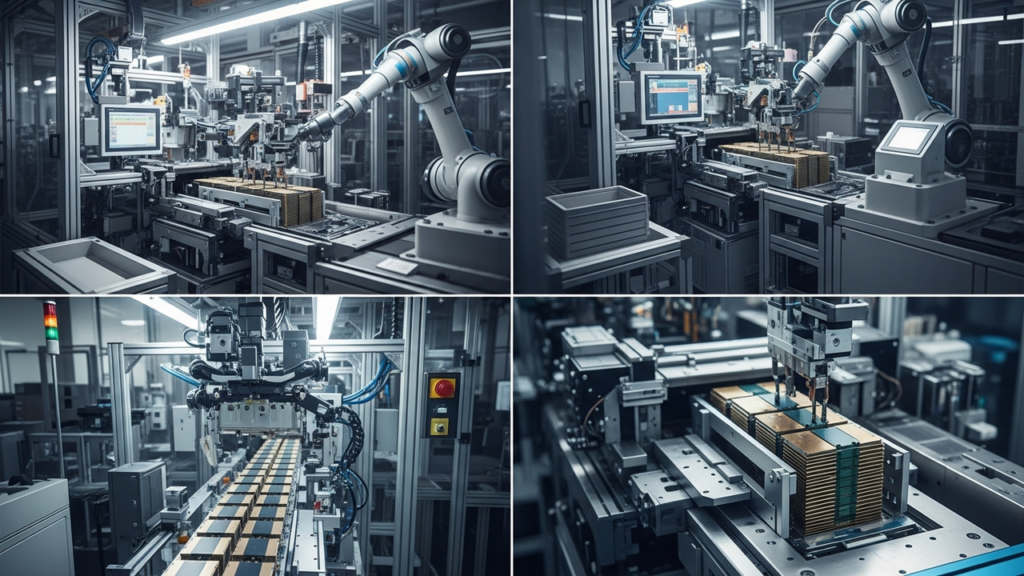
AI CERTs News USA Overview HBM stack manufacturing demands Through Silicon Vias (TSV) and high-precision bonding equipment, with low yield tolerance posing an industry challenge. Limited vendors for these specialized tools mean HANMI, a ... -
JEDEC Relaxes HBM4 Package Height to 775 µm, Enabling 12-Hi/16-Hi Stacks Without Immediate Cu-Cu Hybrid Bonding
Exponential Industry USA Overview JEDEC has relaxed the HBM4 package height specification from 720 µm to 775 µm, allowing for 12-Hi and 16-Hi stack HBM modules without immediate reliance on Cu-Cu hybrid bonding. HBM utilizes 3D stacked D... -
Samsung Delays Hybrid Bonding HBM Mass Production to 2029-2030, Aligning with Technical Challenges and NVIDIA’s Next-Gen GPUs
TrendForce South Korea Overview Samsung Electronics is reportedly delaying the full-scale mass production of its hybrid bonding technology for next-generation HBM and logic semiconductors until 2029-2030. The company is currently buildin... -
HBM Supply Crunch Deepens: DRAM Wafer Production and Advanced Packaging/Test Emerge as Dual Bottlenecks Amid Samsung, SK Hynix, Micron Rivalry
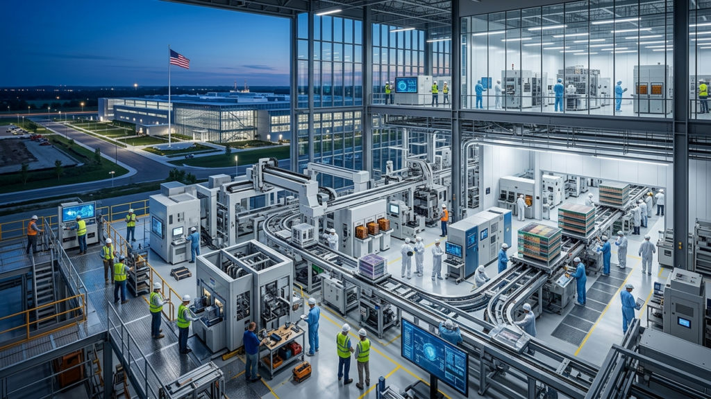
Industry Analysis International Overview High Bandwidth Memory (HBM), central to AI, faces dual bottlenecks in both DRAM wafer manufacturing and advanced packaging/test capacity. HBM achieves high bandwidth and energy efficiency through ... -
Data Insights Reports Forecasts Electronic Circuit Board Underfill Market Growth Driven by Advanced Semiconductor Packaging Demand, Emphasizing Nano-Fillers for Enhanced Thermal Conductivity and Low-Viscosity for Sub-80 µm Bump Pitch
Data Insights Reports India Overview This article is an overview of a market research report provided by Data Insights Reports. The global electronic circuit board underfill market is projected for significant growth, driven by increasin... -
Kynix Explains HBM4 Hybrid Copper Bonding Achieves Over 20% Thermal Performance Improvement, Enabling Stable Clock Speeds Under AI Loads
Kynix China Overview Kynix explains that Hybrid Copper Bonding (HCB) technology for HBM4 improves thermal performance by over 20%. This method eliminates solder bumps and underfill, directly connecting copper layers to significantly redu... -
Imec’s Chiplet Imperative: Analyzing the Transition to High-Bandwidth, Low-Energy AI/HPC Systems
imec ベルギー Overview Imec has published a comprehensive analysis identifying the economic and technical inflection points for transitioning from monolithic ASICs to chiplet-based designs, particularly for AI, HPC, and data center appli... -
Apple’s M5 Ultra Pioneers Integration with TSMC’s N3P Process and SoIC-mH Packaging
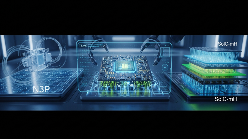
TrendForce Taiwan Overview Reports indicate Apple's upcoming M5 Ultra chip, expected at WWDC, will likely leverage TSMC's N3P process node and its advanced SoIC-mH (System-on-Integrated-Chips – molded horizontal packaging) technology. So...






12