Key Findings
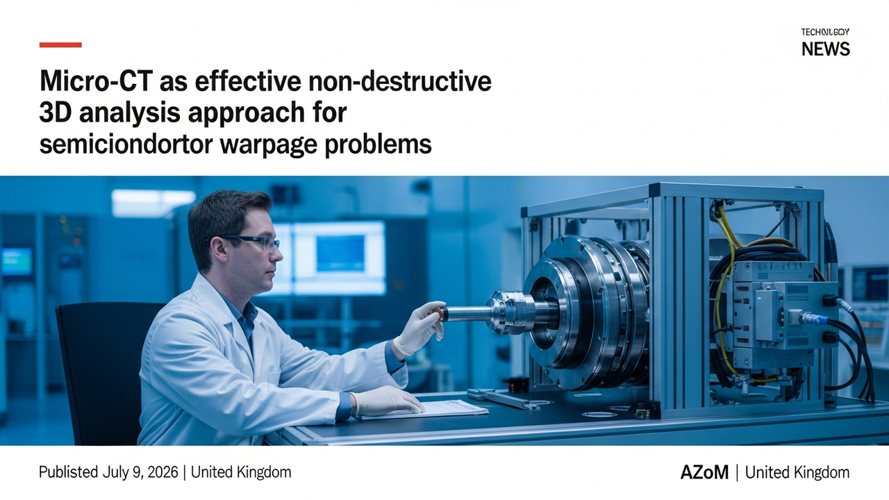
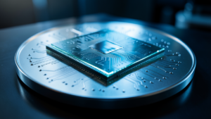
Semiconductor package warpage has emerged as a critical issue that significantly degrades device performance and reliability, with its impact escalating in modern semiconductor manufacturing characterized by miniaturization and high-density integration. This complex deformation is primarily attributed to Coefficient of Thermal Expansion (CTE) mismatches among the various constituent materials within the package (e.g., substrate, silicon chip, molding compound) and thermal/chemical shrinkage of encapsulation materials during curing. In response to this challenge, micro-CT (X-ray micro-tomography) is gaining substantial attention as a highly effective approach for non-destructive, high-resolution, three-dimensional analysis of warpage phenomena within the industry.
Technical/Clinical Details
Micro-CT utilizes X-rays to penetrate a sample, capturing multiple angular projections which are then computer-processed to reconstruct the sample’s internal structure in 3D. This technique allows for detailed visualization of minute deformations and stress distributions within each component of the package—including adhesive layers, underfill materials, molding compounds, substrates, and silicon chips—without destroying the sample. Critically, it enables precise evaluation, from millimeter to micrometer scales, of how CTE mismatches and cure shrinkage, which are root causes of warpage, affect the overall package structure. This provides invaluable data for comparing simulation results with actual warpage behavior during the design phase, aiding in the optimization of material selection and process conditions.
Background & Context
As semiconductor devices become more powerful and miniaturized, packaging technologies grow increasingly complex. In advanced packaging techniques such as flip-chip, SiP (System-in-Package), and TSV (Through-Silicon Via), the high interconnection density between the chip and substrate means even slight warpage can lead to electrical connection failures or degradation in thermal performance. Thermal stresses arising from the stacking of dissimilar materials are an unavoidable problem, and accurately understanding and controlling them is essential for ensuring package reliability. Non-destructive 3D analysis via micro-CT offers deep insights previously unattainable with conventional 2D measurements or destructive testing, contributing to rapid problem-solving and shorter development cycles.
Strategic Significance & Outlook
Micro-CT technology holds the potential to become the de facto standard for semiconductor package warpage analysis. Its application will enable semiconductor manufacturers to rapidly develop more robust and reliable package designs and optimize manufacturing processes. Furthermore, its role will expand in evaluating new material introductions and quality control. In the future, applications in automated defect detection and predictive maintenance, combined with AI, are anticipated to further enhance semiconductor manufacturing efficiency and reliability. This advancement will ultimately lead to the provision of higher-performance and more durable electronic devices for consumers.
Source: https://www.azom.com/article.aspx?ArticleID=25328
Get our weekly technology intelligence — free
Receive an infographic that lets you judge at a glance whether each field’s analysis report is worth reading.
Subscribe Free — Weekly Tech Intelligence
By subscribing, you’ll receive Troy-Technical’s weekly technology intelligence newsletter.
- Your email and selected fields are used only to deliver the newsletter.
- We never share your information with third parties.
- You can unsubscribe anytime via the link in each email.
See our Privacy Policy for details.
Takes about a minute · Unsubscribe anytime




Comments