Key Findings
Fueled by the explosive growth of AI workloads, the semiconductor industry is undergoing a dramatic shift, moving beyond the confines of traditional System-on-Chip (SoC) designs towards Heterogeneous Large-Scale Integration (HLSI). This paradigm shift is being enabled by significant advancements in 3D integration and hybrid bonding, which allow for high-density connections of multiple functional dies within a single package, delivering near-monolithic performance. TSMC’s Co-Packaged Optics (CPO) technology, now in production, is fundamentally redefining high-performance computing design for the AI era by bringing optical interconnects closer to the processor, as copper wiring approaches its inherent limits in bandwidth and power consumption.
Technical / Clinical Details
HLSI represents an approach where multiple functional chiplets (e.g., CPU, GPU, memory, I/O), fabricated using different process technologies, are integrated into a single system using advanced packaging. This allows individual chiplets to be manufactured with processes optimized for their specific function, thereby balancing performance, cost, and power efficiency. 3D integration technology vertically stacks chiplets and connects them using Through-Silicon Vias (TSVs), drastically shortening wiring lengths and boosting bandwidth. Furthermore, hybrid bonding is a direct chip-to-chip connection technology that uses fine copper-to-copper bonds, offering higher density and superior electrical performance compared to conventional micro-bump bonding. This effectively elevates inter-die connection density to a near-monolithic level.
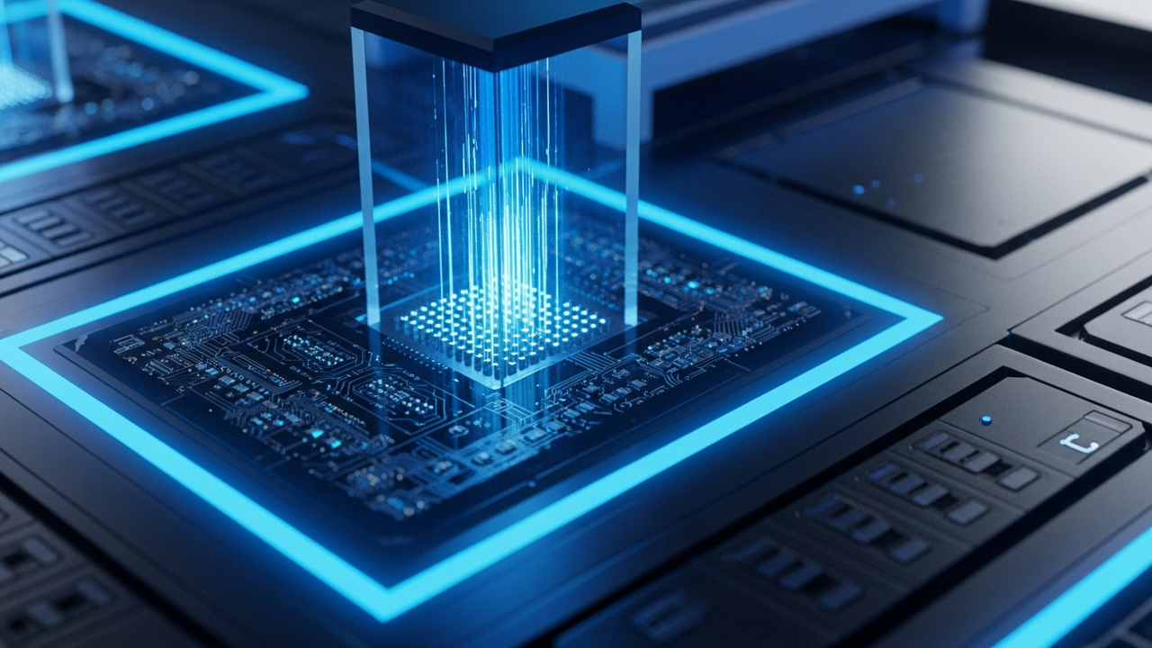
TSMC’s Co-Packaged Optics (CPO) technology is a crucial innovation for addressing I/O bottlenecks in AI/HPC systems. In traditional systems, processors and optical modules existed separately, connected by electrical signals. However, as AI chip performance increases, electrical interconnects hit data transfer speed limits and increased power consumption. CPO directly integrates optical interconnects within the processor package, shortening the distance for electrical-to-optical signal conversion, achieving ultra-high-speed data transmission and significant power efficiency improvements. This enables a dramatic increase in connection bandwidth between AI clusters in data centers.
Background & Context
The deceleration of Moore’s Law prompted the semiconductor industry to seek new ways to improve chip performance and reduce costs. The immense data processing capabilities and low latency required by fields such as AI, data centers, and 5G/6G communication can no longer be met by traditional SoC approaches alone. HLSI and chiplets have emerged as powerful solutions to this challenge, leading to the development of various advanced packaging technologies like Intel’s EMIB, Samsung’s I-Cube, and TSMC’s CoWoS/SoIC. CoWoS, in particular, has been widely adopted in Nvidia’s AI accelerators, becoming a de facto standard for AI chip design. The introduction of CPO signifies a new phase where I/O bottlenecks constrain overall system performance, implying that optical technology is becoming an indispensable component of semiconductor packaging.
Strategic Significance & Outlook
The shift towards HLSI will continue to fundamentally redefine semiconductor industry design and manufacturing for years to come. With increasing complexity of AI workloads and data volumes, the demand for higher-density and more efficient chip integration will only grow. Technologies like 3D integration, hybrid bonding, and Co-Packaged Optics are key to pushing the boundaries of AI performance, enabling new applications and services. This trend fosters collaboration and innovation across the entire semiconductor ecosystem, from chip designers to packaging engineers, material scientists, and manufacturing equipment suppliers. The commencement of CPO mass production will significantly impact AI data center architectures, contributing to the realization of more energy-efficient, high-performance computing infrastructure. HLSI is not just a technical advancement, but a strategic turning point for the semiconductor industry to overcome physical and economic constraints and build the foundation for next-generation computing.
Source: https://www.nextmsc.com/news/chiplet-market-pivots-to-hlsi-as-ai-reshapes-chip-design
Get our weekly technology intelligence — free
Receive an infographic that lets you judge at a glance whether each field’s analysis report is worth reading.
Subscribe Free — Weekly Tech Intelligence
By subscribing, you’ll receive Troy-Technical’s weekly technology intelligence newsletter.
- Your email and selected fields are used only to deliver the newsletter.
- We never share your information with third parties.
- You can unsubscribe anytime via the link in each email.
See our Privacy Policy for details.
Takes about a minute · Unsubscribe anytime









Comments