Key Findings
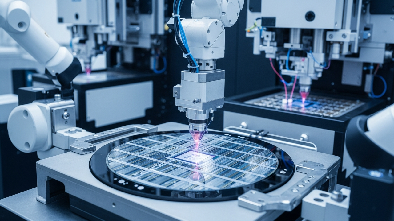
Applied Materials underscores the paramount importance of material engineering innovations, including its ‘Kinex’ hybrid bonding system, for achieving exponential leaps in chip performance within the Artificial Intelligence (AI) era. The company views advanced packaging technologies that efficiently integrate multiple chiplets, delivering higher bandwidth and superior energy efficiency, as foundational to next-generation AI infrastructure.
Technical and Clinical Details
Applied Materials identifies five core areas defining AI system architecture: 1. Leading-edge logic, 2. High-performance DRAM, 3. HBM (High Bandwidth Memory), 4. Advanced packaging, and 5. Power electronics. Breakthroughs in materials engineering are indispensable across all these domains. For instance, to support the scaling of Gate-All-Around (GAA) transistors at 2nm and beyond, innovative thin-film technologies, such as Applied Materials’ ‘Xtera’ epitaxy system, are crucial. Hybrid bonding technology, by directly and electrically connecting different chiplets, achieves significantly higher interconnection density and shorter wiring distances compared to conventional microbumps, dramatically improving data transfer speeds and energy efficiency. Precise thin-film deposition, patterning, and inspection techniques are essential to ensure the manufacturing yield and reliability of these advanced structures.
Background and Industry Context
The increasing complexity of AI models and the explosion in data volume demand unprecedented computational power and efficiency from semiconductor chips. Traditional chip design struggles to meet these requirements, leading to a prevalent shift towards ‘heterogeneous integration’ via chiplets and advanced packaging technologies. In this new architectural paradigm, not only the miniaturization of individual chips but also how efficiently and power-consciously they are interconnected has become a new differentiator for AI chip performance. Applied Materials, leveraging its expertise in materials science and process technology, is at the forefront of providing equipment and solutions to address this evolving landscape in semiconductor manufacturing.
Strategic Significance and Outlook
The material engineering and advanced packaging innovations championed by Applied Materials are pivotal for scaling AI chip performance. The widespread adoption of hybrid bonding technology is set to revolutionize the design and manufacturing of AI accelerators, HPC, and future physical AI (edge AI) devices. The company’s solutions pave the way for semiconductor manufacturers to implement GAA transistors at 2nm and beyond process nodes and mass-produce increasingly complex 3D packaging structures. This will accelerate the further evolution and adoption of AI technologies, leading to substantial economic and social impacts across a wide range of industries.
Source: https://www.appliedmaterials.com/jp/ja/the-ai-era.html
Get our weekly technology intelligence — free
Receive an infographic that lets you judge at a glance whether each field’s analysis report is worth reading.
Subscribe Free — Weekly Tech Intelligence
By subscribing, you’ll receive Troy-Technical’s weekly technology intelligence newsletter.
- Your email and selected fields are used only to deliver the newsletter.
- We never share your information with third parties.
- You can unsubscribe anytime via the link in each email.
See our Privacy Policy for details.
Takes about a minute · Unsubscribe anytime









Comments