Key Findings
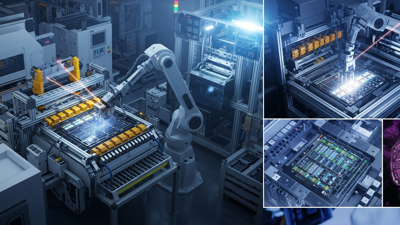
Applied Materials has launched seven innovative semiconductor manufacturing systems aimed at resolving critical bottlenecks in AI chip production, with a focus on DRAM performance scaling and advanced 3D packaging. These new systems are designed to improve yields in high-bandwidth memory (HBM) and chiplet-based designs, thereby facilitating the high-performance demands of AI chips.
Technical and Clinical Details
The newly introduced suite of systems addresses two primary domains. For DRAM performance scaling, an enhanced Centura Prime Epi epitaxy system has been developed. This system optimizes crucial film deposition processes in DRAM manufacturing, contributing to the performance improvement of next-generation memory. For advanced packaging, three pivotal process tools have been introduced: The Opta Quad CMP system is engineered for chemical mechanical planarization (CMP), a critical step for hybrid bonding technology, ensuring exceptional flatness and uniformity. The Nokota VMax 2 electrochemical deposition system enables high-precision copper filling for Through-Silicon Vias (TSVs) and microbumps. Additionally, two eBeam systems, including the VeritySEM 7AP, provide critical dimension (CD) metrology on heterogeneous substrates, guaranteeing the accuracy and quality of complex 3D structures. These tools directly contribute to optimizing fine interconnections and yields, which are major challenges in HBM and chiplet integration.
Background and Industry Context
The explosive growth of AI has made high-performance CPUs, GPUs, and high-capacity, high-bandwidth memory (HBM) indispensable. These AI chips necessitate advanced packaging technologies that integrate multiple distinct chiplets and HBM stacks beyond mere transistor density. However, this intricate packaging process has emerged as a new manufacturing bottleneck, characterized by challenges in fine interconnections, thermal management, and yield optimization. Applied Materials’ new systems directly confront these challenges, aiming to expand AI chip manufacturing capabilities from the perspectives of materials engineering and process technology.
Strategic Significance and Outlook
These innovative systems from Applied Materials are poised to be crucial enablers for accelerating AI chip performance enhancement and mass production. Advanced technologies like hybrid bonding and TSVs are particularly important for significantly improving interconnection density and efficiency between chiplets, essential for next-generation AI accelerators and data center processors. These tools not only refine existing processes but also establish new benchmarks for semiconductor manufacturing in the AI era, paving the way for the realization of more complex and higher-performing chip designs, thereby exerting a significant impact across the industry.
Get our weekly technology intelligence — free
Receive an infographic that lets you judge at a glance whether each field’s analysis report is worth reading.
Subscribe Free — Weekly Tech Intelligence
By subscribing, you’ll receive Troy-Technical’s weekly technology intelligence newsletter.
- Your email and selected fields are used only to deliver the newsletter.
- We never share your information with third parties.
- You can unsubscribe anytime via the link in each email.
See our Privacy Policy for details.
Takes about a minute · Unsubscribe anytime









Comments