Key Findings
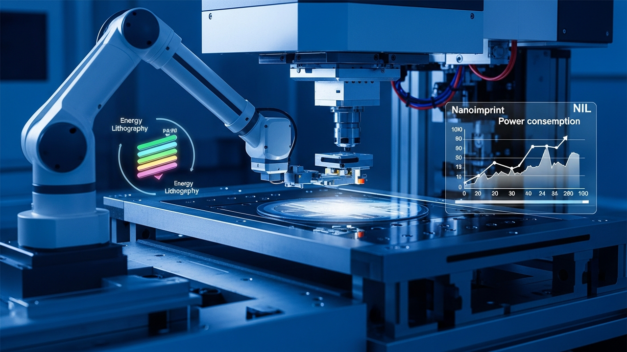
Dai Nippon Printing (DNP) has unveiled its advanced Nanoimprint Lithography (NIL) technology, establishing a capability for intricate pattern formation essential for high-performance semiconductors. This innovative process holds the potential to reduce the power consumption of semiconductor exposure processes by approximately a factor of ten compared to conventional methods, positioning it as a pivotal solution for both advanced miniaturization and environmental sustainability in chip manufacturing.
Technical / Clinical Details
Nanoimprint Lithography operates on a fundamentally different principle than optical lithography, enabling the creation of nanoscale circuit patterns. The NIL process begins with the preparation of a template featuring the desired circuit design as a surface relief pattern. This template is then directly pressed into a resin-coated semiconductor substrate. Following the imprinting, ultraviolet (UV) light is exposed to cure the resin, permanently transferring the template’s pattern onto the substrate’s resin layer. This physical replication method facilitates the formation of extremely fine nanoscale patterns. A primary advantage of NIL is its elimination of complex optical systems, leading to simpler equipment and significantly reduced manufacturing costs compared to traditional optical lithography. Furthermore, the absence of high-power laser sources for exposure dramatically lowers energy consumption. DNP’s NIL technology has achieved high levels of pattern transfer accuracy and uniformity, capable of supporting sub-10nm feature sizes required for cutting-edge semiconductor devices. This precision and efficiency pave the way for the mass production of more powerful and energy-efficient semiconductors.
Background & Context
The semiconductor industry is currently grappling with the physical and economic limits of Moore’s Law, with conventional optical lithography facing escalating costs and power consumption issues. Extreme Ultraviolet (EUV) lithography, while pushing miniaturization, demands extremely expensive and complex equipment and consumes vast amounts of energy to operate. Against this backdrop, NIL emerges as a compelling alternative or complementary technology to EUV, offering a cost-effective and energy-efficient solution for advanced patterning. DNP, leveraging its extensive expertise in microfabrication and materials science, is positioning itself as a leader in the NIL domain.
Strategic Significance & Outlook
DNP’s NIL technology is expected to gain increasing importance as demand for high-performance, low-power semiconductors grows, particularly for data centers, AI chips, and IoT devices. In the future, NIL is anticipated to coexist with EUV lithography, demonstrating superiority in specific applications within memory, logic, and other specialized semiconductor device manufacturing. DNP aims to drive the further practical implementation and widespread adoption of NIL by advancing comprehensive efforts from template manufacturing to equipment development and process optimization. This trajectory holds significant promise for greening semiconductor production and enabling the realization of next-generation electronic devices.
Source: https://www.global.dnp/en/biz/solution/semiconductors/10162425/
Get our weekly technology intelligence — free
Receive an infographic that lets you judge at a glance whether each field’s analysis report is worth reading.
Subscribe Free — Weekly Tech Intelligence
By subscribing, you’ll receive Troy-Technical’s weekly technology intelligence newsletter.
- Your email and selected fields are used only to deliver the newsletter.
- We never share your information with third parties.
- You can unsubscribe anytime via the link in each email.
See our Privacy Policy for details.
Takes about a minute · Unsubscribe anytime






Comments