Key Findings
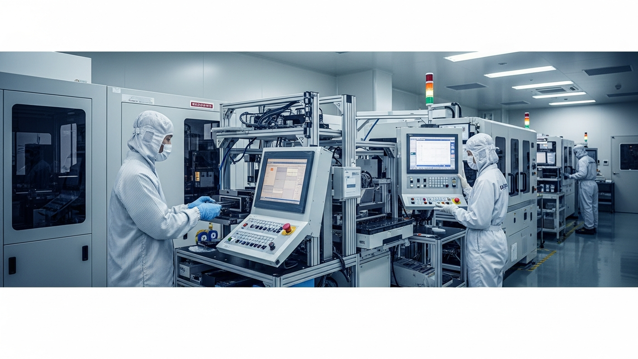
Japan’s Rapidus, with substantial financial backing from both government and private sectors, is driving a national project to establish domestic advanced semiconductor manufacturing using the 2nm (nanometer) process. The company aims to commence mass production of Artificial Intelligence (AI) chips by 2027, an endeavor expected to stimulate significant demand for manufacturing equipment and materials across Japan’s entire semiconductor industry ecosystem.
Technical and Clinical Details
Rapidus’ 2nm plan necessitates the integration of cutting-edge front-end processes such as Extreme Ultraviolet (EUV) lithography, Atomic Layer Deposition (ALD), high-precision etching, advanced cleaning, and stringent inspection technologies, alongside advanced packaging. AI chips are increasingly adopting ‘chiplet architectures’ to achieve high performance by combining multiple smaller functional units. This approach requires wafer thinning, hybrid bonding, high-density interconnections, precise planarization, and comprehensive inspection. Applied Materials, in June 2026, unveiled new semiconductor manufacturing systems designed for AI chip DRAM and advanced packaging. These systems specialize in the production of HBM (High Bandwidth Memory) and complex 3D architectures, aiming to resolve technical challenges in back-end processes such as wafer thinning, chip bonding, fine interconnection formation, chemical mechanical planarization (CMP), and advanced defect inspection.
Background and Industry Context
In response to escalating geopolitical risks and global calls for more resilient semiconductor supply chains, nations are focusing on strengthening their domestic semiconductor manufacturing capabilities. Japan, aiming to regain its past prominence in the semiconductor industry, is pursuing a national strategy centered around Rapidus. Amidst the explosive growth in AI chip demand, cutting-edge technologies like the 2nm process are critically important for ensuring national economic security and technological superiority. Furthermore, AI chip performance improvements are increasingly dependent not only on front-end miniaturization but also on back-end advanced packaging, prompting equipment manufacturers like Applied Materials to accelerate product development in response to this market shift.
Strategic Significance and Outlook
Rapidus’ 2nm process development and mass production target are expected to revitalize Japan’s semiconductor industry and enhance its presence in the global supply chain. Collaboration with IBM on advanced packaging technology will further strengthen its competitiveness. This initiative is also anticipated to generate significant ripple effects across Japan’s semiconductor materials and equipment industries, leading to accelerated R&D investments and new job creation. Coupled with technological innovations from global equipment manufacturers like Applied Materials, AI-era semiconductor manufacturing will evolve into an even more complex and integrated process. Rapidus’ success is thus deemed to hold strategic significance in contributing to the establishment of a resilient Indo-Pacific semiconductor ecosystem.
Source: https://www.datamintelligence.com/blogs/semiconductor-manufacturing-equipment-ai-usa-japan
Get our weekly technology intelligence — free
Receive an infographic that lets you judge at a glance whether each field’s analysis report is worth reading.
Subscribe Free — Weekly Tech Intelligence
By subscribing, you’ll receive Troy-Technical’s weekly technology intelligence newsletter.
- Your email and selected fields are used only to deliver the newsletter.
- We never share your information with third parties.
- You can unsubscribe anytime via the link in each email.
See our Privacy Policy for details.
Takes about a minute · Unsubscribe anytime









Comments