Key Findings
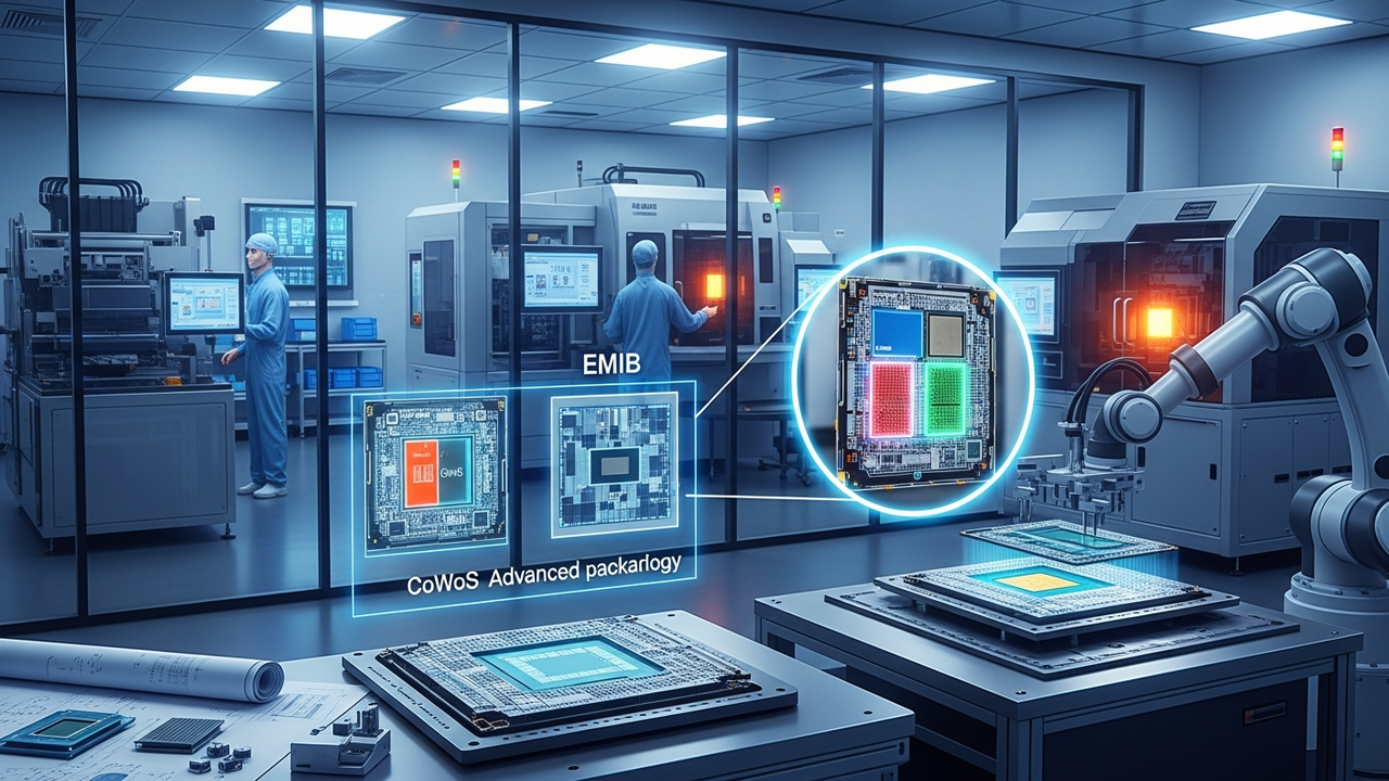
The advanced packaging segment, specifically TSMC’s CoWoS technology, has emerged as a critical bottleneck in AI chip production, leading industry giant NVIDIA to reportedly explore Intel’s EMIB (Embedded Multi-die Interconnect Bridge) for its future GPU manufacturing. This development underscores the escalating pressure on the semiconductor backend, where AI’s insatiable demand for high-performance, integrated solutions is outpacing the supply of specialized packaging capabilities. The strategic diversification by a leading AI hardware developer signals a pivotal moment in the supply chain dynamics for artificial intelligence.
Technical & Business Details
- NVIDIA’s reported interest in Intel’s EMIB represents a significant potential shift, as EMIB offers an alternative to CoWoS for integrating multiple dies from different process nodes within a single package. This move could provide NVIDIA with increased supply chain flexibility and mitigate risks associated with the tight CoWoS capacity, fostering a more robust and resilient production ecosystem.
- Leading Outsourced Semiconductor Assembly and Test (OSAT) providers are responding with substantial investments globally. Taiwan’s ASE Technology projects its advanced packaging revenue will exceed $3.5 billion in 2026, marking a 10% year-over-year growth, driven primarily by robust AI and high-performance computing (HPC) demand.
- In the United States, Amkor Technology has announced a $7 billion investment to construct a new advanced packaging and testing complex in Peoria, Arizona, with initial production slated for early 2028. This strategic expansion is designed to support AI, HPC, communications, automotive, and industrial applications, bolstering the domestic semiconductor supply chain.
- Japan’s Ibiden anticipates significant growth in IC substrate demand for AI servers, projecting substantial expansion by 2030 and planning approximately 500 billion JPY (around $3.2 billion USD) in capital expenditure through 2028 for high-performance IC package substrate capacity. Ajinomoto, another Japanese firm, continues to dominate the ABF (Ajinomoto Build-up Film) market, holding over 95% share for advanced IC package substrate dielectric materials, crucial for AI chip performance.
- In the memory sector, South Korea’s SK Hynix has advanced its MR-MUF (Mass Reflow Molded Underfill) process for HBM4E, achieving a 17% reduction in thermal resistance. This innovation is vital for managing the increased heat generated by high-density HBM stacks, crucial for the reliability and performance of next-generation AI accelerators.
Background & Context
The rapid advancement of AI models necessitates not only cutting-edge CPU and GPU processing power but also highly efficient integration of these components with high-bandwidth memory (HBM). This integration, particularly through 2.5D and 3D packaging technologies like CoWoS, has become as critical as leading-edge wafer fabrication. The current bottleneck is a direct consequence of this integrated demand, pushing the entire semiconductor industry to accelerate investments in backend processes, materials, and testing capabilities.
Strategic Significance & Outlook
The escalating demand for AI chips is expected to drive exponential growth in advanced packaging technologies and associated materials and equipment. NVIDIA’s consideration of Intel’s EMIB signals a strategic push towards diversifying supply chains and mitigating risks from concentrated capacity. This suggests a future where multiple advanced packaging solutions coexist, each optimized for specific applications and supply chain resilience. Further innovations in next-generation substrate technologies, such as glass substrates, and advancements in HBM thermal management will be crucial for enhancing AI hardware performance and cost-efficiency. The interplay of competition and collaboration in these areas will shape the future trajectory of the semiconductor industry.
Source: https://economy.ac/news/2026/07/202607289543
Get our weekly technology intelligence — free
Receive an infographic that lets you judge at a glance whether each field’s analysis report is worth reading.
Subscribe Free — Weekly Tech Intelligence
By subscribing, you’ll receive Troy-Technical’s weekly technology intelligence newsletter.
- Your email and selected fields are used only to deliver the newsletter.
- We never share your information with third parties.
- You can unsubscribe anytime via the link in each email.
See our Privacy Policy for details.
Takes about a minute · Unsubscribe anytime









Comments