Key Findings
Chinese technology firm HKC has announced a significant investment of 4 billion RMB (approximately $550 million USD) in an advanced semiconductor packaging and test project in the Shaoxing Economic Development Zone. This move marks a strategic expansion aimed at bolstering China’s domestic semiconductor supply chain and addressing the increasing demand for advanced chip packaging and testing services, particularly for heterogeneous chip integration.
Technical & Manufacturing Details
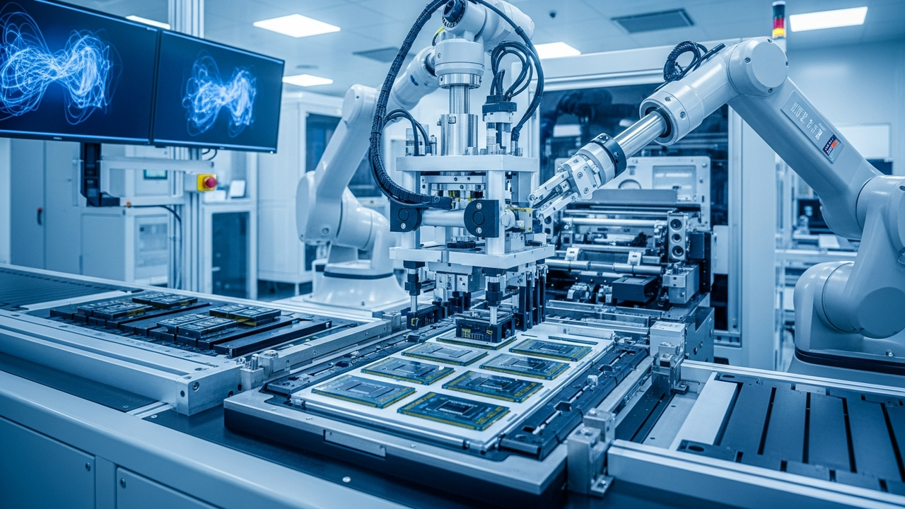
Through its newly established subsidiary, Zhejiang Huaxin Advanced Semiconductor Co. Ltd., HKC will construct a 12-inch advanced packaging and test line specifically designed for heterogeneous chip integration. The project is planned in two phases, ultimately targeting a monthly production capacity of 20 million units. Heterogeneous integration involves combining diverse chiplets—such as logic, memory, and sensors—into a single package, enabling enhanced performance, reduced power consumption, and improved cost efficiency. This capability is crucial for meeting the stringent demands of applications in AI, 5G, and HPC (High-Performance Computing).
The facility will focus on:
- **12-inch Wafer Processing:** Implementing state-of-the-art 12-inch wafer processing lines to ensure high-efficiency manufacturing.
- **Heterogeneous Integration Specialization:** Concentrating on integrating different types of chips into a single, high-performance package.
- **Robust Testing Capabilities:** Establishing advanced testing protocols to guarantee the reliability and quality of integrated circuits.
Background & Context
The global semiconductor industry has recently seen an acceleration in efforts by various nations to enhance their domestic manufacturing capabilities, driven by geopolitical considerations and the desire for supply chain resilience. China is a key player in this trend, with its government actively promoting self-sufficiency and technological innovation in the semiconductor sector. HKC’s investment is a direct manifestation of this national strategy, aiming to improve China’s competitiveness in advanced packaging, a field where Taiwan and South Korea currently hold significant leads. The goal is to reduce reliance on external suppliers and achieve greater technological independence by strengthening domestic capabilities across design, manufacturing, packaging, and testing.
Strategic Significance & Outlook
This new advanced packaging and test facility is expected to accelerate the development and production of chips for AI and HPC applications within China. The ambitious monthly production capacity of 20 million units will not only cater to domestic demand but also has the potential to elevate China’s position in the global semiconductor supply chain. By focusing on heterogeneous chip integration, HKC is aligning itself with a pivotal trend in future high-performance semiconductor design, laying a robust foundation to become a significant player in this critical technological domain.
Get our weekly technology intelligence — free
Receive an infographic that lets you judge at a glance whether each field’s analysis report is worth reading.
Subscribe Free — Weekly Tech Intelligence
By subscribing, you’ll receive Troy-Technical’s weekly technology intelligence newsletter.
- Your email and selected fields are used only to deliver the newsletter.
- We never share your information with third parties.
- You can unsubscribe anytime via the link in each email.
See our Privacy Policy for details.
Takes about a minute · Unsubscribe anytime









Comments