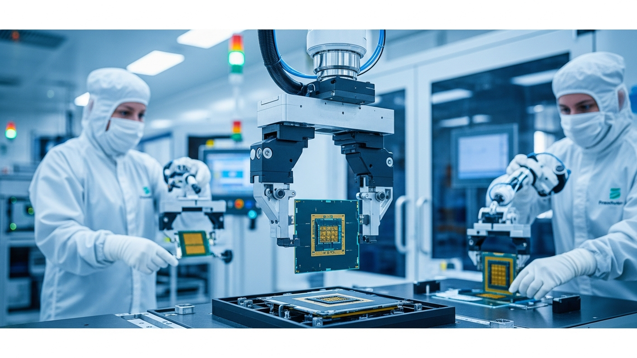
Strategic Context: Bolstering Europe’s Semiconductor Future
Driven by escalating geopolitical risks within global semiconductor supply chains and the surging demand for artificial intelligence (AI) and high-performance computing (HPC) capabilities, the European Union enacted the EU Chips Act. This comprehensive legislative framework is designed to significantly enhance Europe’s domestic semiconductor manufacturing capacity and research and development prowess. Within this overarching strategy, advanced packaging and heterogeneous integration are recognized as pivotal enablers for boosting semiconductor performance, particularly as traditional transistor scaling approaches encounter diminishing returns. The establishment of specialized pilot lines by leading research institutions such as Fraunhofer is therefore an indispensable step for Europe to cultivate global competitiveness and forge a resilient, self-sufficient technological ecosystem in this strategically vital sector.
Key Developments
The Fraunhofer Institute for Applied Solid State Physics (IAF) has officially launched APECS (Advanced Packaging for Electronic Components and Systems), a pioneering pilot line dedicated to advanced packaging and heterogeneous integration technologies for electronic components and systems. Operating under the framework of the EU Chips Act, this strategic initiative aims to significantly strengthen Europe’s semiconductor industry. The cutting-edge platform offers comprehensive support across the entire product lifecycle, from the initial development and sophisticated integration of next-generation microelectronic systems to their pilot-scale manufacturing, thereby fast-tracking the commercialization of research breakthroughs into industrial applications.
Technical Deep Dive
- APECS Platform Objectives: The APECS pilot line is engineered to bolster Europe’s technological sovereignty in electronic component packaging and heterogeneous integration – the seamless integration of chips with diverse functionalities. This state-of-the-art facility will function as a shared, open-access resource, enabling researchers and industrial partners to collaboratively develop, rigorously test, and conduct low-volume production of novel, high-performance packaging solutions.
- Advancing Heterogeneous Integration: A core focus of the pilot line will be on pioneering technologies for integrating chiplets—manufactured on disparate process nodes—into a single, unified package. This innovative approach allows for the synergistic combination of the optimal performance characteristics of individual chips, leading to the creation of significantly more complex and higher-performing systems. This capability is particularly crucial for emerging applications in high-frequency electronics, quantum computing, and other advanced domains.
- Groundbreaking Panel-Level Fan-Out Packaging (FOPLP) Demonstration: A significant early achievement within the APECS platform saw Fraunhofer IZM successfully demonstrate panel-level fan-out packaging (FOPLP) on impressively large panels, measuring up to 610 x 457 mm. This represents a paradigm shift in packaging technology, promising substantial cost reductions and dramatic throughput improvements compared to conventional circular wafer-based manufacturing. This breakthrough is poised to accelerate the industry’s critical transition towards large-area, high-throughput advanced packaging solutions.
Strategic Impact and Future Outlook
The inauguration of the APECS pilot line is set to dramatically accelerate the advancement of critical packaging technologies within Europe’s burgeoning semiconductor industry. This strategic asset will empower European enterprises to engineer more innovative, robust, and reliable microelectronic systems tailored for strategically vital sectors, including artificial intelligence (AI), 5G/6G communications, advanced automotive systems, and industrial Internet of Things (IoT) applications. For researchers and engineers across the continent, APECS expands unprecedented opportunities for collaborative research and rapid prototype development utilizing cutting-edge facilities. Furthermore, for investors, the robust policy support enshrined in the EU Chips Act, coupled with the groundbreaking technological innovations spearheaded by institutions like Fraunhofer, collectively signal compelling new investment opportunities within the dynamic European semiconductor ecosystem.
Get our weekly technology intelligence — free
Receive an infographic that lets you judge at a glance whether each field’s analysis report is worth reading.
Subscribe Free — Weekly Tech Intelligence
By subscribing, you’ll receive Troy-Technical’s weekly technology intelligence newsletter.
- Your email and selected fields are used only to deliver the newsletter.
- We never share your information with third parties.
- You can unsubscribe anytime via the link in each email.
See our Privacy Policy for details.
Takes about a minute · Unsubscribe anytime









Comments