Key Findings
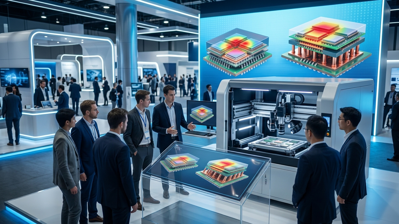
Koh Young Technology is slated to participate in the 37th Annual Electronics Packaging Symposium (EPS 2026), where it will address complex measurement challenges associated with advanced packaging in critical areas such as AI, chiplet-based architectures, heterogeneous integration, and thermal management. The company will emphasize its high-resolution 3D measurement and AI-driven inspection solutions, exemplified by its Meister Series and ZenStar platforms, as essential tools for ensuring the quality and reliability of next-generation semiconductor packaging.
Technical / Clinical Details
At EPS 2026, Koh Young will particularly focus on challenges faced by cutting-edge semiconductor packaging technologies, including high-bandwidth memory (HBM) and AI-oriented packaging like CoWoS™ (Chip-on-Wafer-on-Substrate). These packaging architectures feature extremely fine solder bumps, tight gaps, and intricate multi-layered structures, making the detection of subtle defects — often missed by conventional 2D inspection — absolutely critical. The Meister Series and ZenStar platforms leverage high-precision 3D measurement technology to non-contactually assess detailed geometric characteristics such as volume, shape, and position of these minuscule interconnects. Furthermore, these AI-powered systems analyze inspection data in real-time, automatically identifying and classifying potential defects that could impact yield. This capability enables early detection of issues in the manufacturing process, minimizing scrap, and enhancing overall production efficiency and product reliability.
Background & Context
The rapid advancements in AI, 5G, and autonomous driving technologies have placed unprecedented demands not only on semiconductor chip performance but also on the underlying packaging technologies. Specifically, chiplets and heterogeneous integration, which involve integrating multiple chips into a single package, require larger package sizes, finer Redistribution Layers (RDLs), and efficient thermal management. In such complex package structures, even minute manufacturing defects can significantly impact overall performance and reliability, making high-precision measurement and inspection indispensable. As a long-standing leader in 3D measurement technology, Koh Young has contributed significantly to the semiconductor and electronics manufacturing industries, and its technologies have evolved to meet these new challenges.
Strategic Significance & Outlook
Koh Young’s advanced measurement and inspection solutions will play a vital role in realizing the manufacturing reality of semiconductor packaging that underpins AI and next-generation computing. The integrated approach of high-resolution 3D measurement and AI streamlines quality control for increasingly complex packaging structures, contributing to shorter development cycles and cost reductions. Moving forward, the company is expected to further enhance its focus on data-driven intelligent manufacturing, optimizing entire production processes. Through continuous technological innovation, Koh Young aims to remain at the forefront of the industry, adapting to the evolution of new packaging technologies and materials.
Get our weekly technology intelligence — free
Receive an infographic that lets you judge at a glance whether each field’s analysis report is worth reading.
Subscribe Free — Weekly Tech Intelligence
By subscribing, you’ll receive Troy-Technical’s weekly technology intelligence newsletter.
- Your email and selected fields are used only to deliver the newsletter.
- We never share your information with third parties.
- You can unsubscribe anytime via the link in each email.
See our Privacy Policy for details.
Takes about a minute · Unsubscribe anytime






Comments