Key Findings
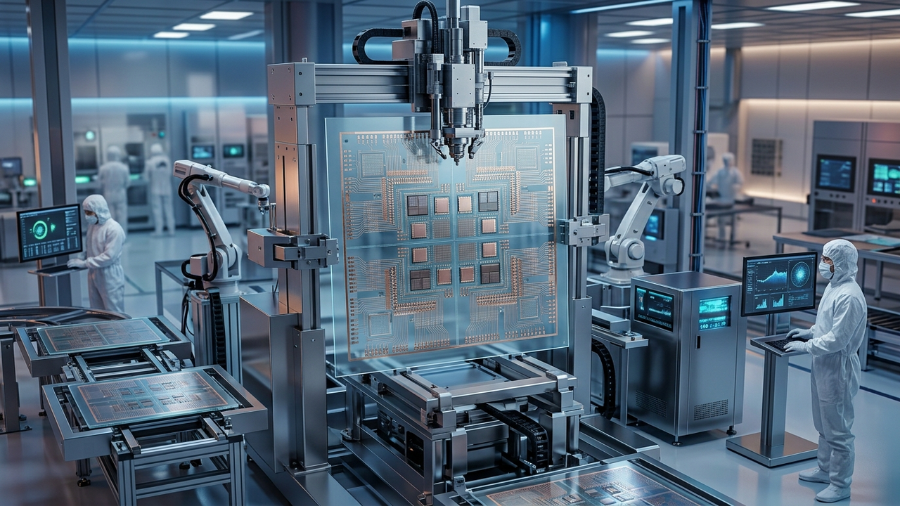
Rapidus, Japan’s leading-edge semiconductor foundry, has outlined an aggressive development roadmap targeting the production of 8-reticle interposers on 600mm advanced packaging panels by 2030. This ambitious goal represents a critical step forward in high-density chiplet integration, promising a substantial boost in performance and density for future high-performance computing (HPC) and artificial intelligence (AI) systems.
Technical / Clinical Details
- 8-Reticle Interposer Scale: While current interposer technologies typically involve smaller panel sizes and fewer reticles, Rapidus’s target of 8 reticles on a 600mm panel significantly scales up the integration capability. This expansive platform will allow for the efficient connection of numerous complex chiplets, including CPUs, GPUs, memory, and critically, future photonic integrated circuits (PICs).
- 600mm Panel Utilization: The adoption of 600mm panels for advanced packaging is driven by the need for enhanced cost efficiency and throughput. Larger panels enable the production of more interposers and final packaged units per manufacturing run, leading to economies of scale and improved productivity, which are vital for meeting the escalating demands of the semiconductor industry.
- Advancing Heterogeneous Integration: This technology is a cornerstone for heterogeneous integration, allowing different functional chiplets to be combined into a single package. For AI and HPC, where bandwidth and power efficiency are paramount, advanced packaging that can seamlessly merge electronic and optical components is indispensable.
Background & Context
The rapid proliferation of AI and the increasing demands of HPC have pushed conventional monolithic semiconductor manufacturing approaches to their limits. Chiplet technology, coupled with advanced packaging, has emerged as a strategic pathway to balance performance, power efficiency, and cost by combining individually optimized chip components. Rapidus’s initiative is part of Japan’s national strategy to regain competitive edge in leading-edge semiconductor manufacturing, with a particular focus on supplying the U.S. HPC market. This technology is expected to directly address the data processing bottlenecks in the AI era.
Strategic Significance & Outlook
Achieving Rapidus’s 2030 goal will provide the foundational technology for next-generation AI accelerators, data center processors, supercomputers, and other high-density, high-performance computing systems. As optical technologies like silicon photonics advance, interposers will increasingly serve as crucial hubs for opto-electronic conversion modules and optical interconnects. This advanced packaging technology is not merely about linking chips; it aims to dramatically expand data transfer bandwidth and enhance system energy efficiency, thereby transforming the entire computing architecture for the AI era. Rapidus’s success in this area could cement Japan’s role as a key player in the global semiconductor advanced packaging landscape.
Source: #
Get our weekly technology intelligence — free
Receive an infographic that lets you judge at a glance whether each field’s analysis report is worth reading.
Subscribe Free — Weekly Tech Intelligence
By subscribing, you’ll receive Troy-Technical’s weekly technology intelligence newsletter.
- Your email and selected fields are used only to deliver the newsletter.
- We never share your information with third parties.
- You can unsubscribe anytime via the link in each email.
See our Privacy Policy for details.
Takes about a minute · Unsubscribe anytime





Comments