Key Findings
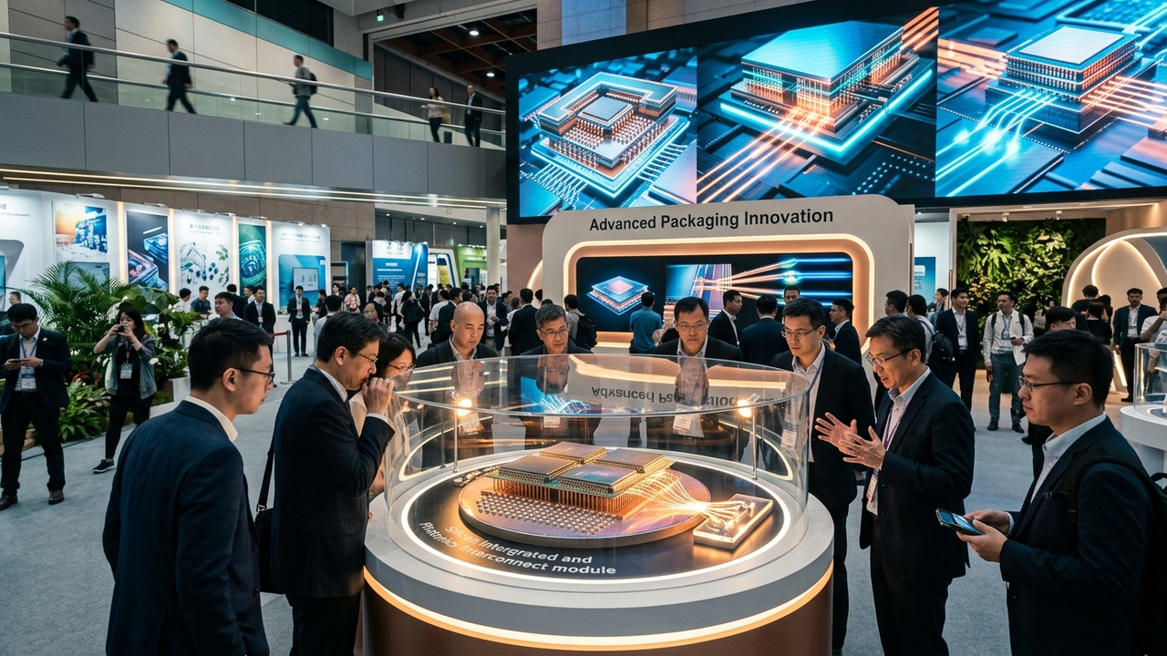
The Advanced Packaging Summit 2026, held concurrently with SEMICON Taiwan from August 31 to September 4, 2026, is a pivotal event dedicated to innovations in advanced packaging within the semiconductor industry. This summit will particularly foster in-depth discussions on cutting-edge advancements in silicon-based integration technologies and photonics-based interconnects, which are poised to significantly enhance packaging productivity and scalability.
Technical Details
Key topics at the summit will include the latest trends in advanced packaging technologies such as chiplet technology, 3D stacking, and heterogeneous integration. Specifically, discussions will cover the characterization and optimization of new materials (e.g., adhesives, encapsulants, thermal interface materials) that underpin these technologies, as well as challenges and solutions in their manufacturing processes. Photonics-based interconnect technologies, critical for achieving dramatic increases in data communication speeds, will also be a major focus, particularly their progress towards practical application in AI and High-Performance Computing (HPC) applications. These technologies are key to overcoming the limitations of traditional Moore’s Law scaling and improving overall system performance and power efficiency.
Background & Context
The semiconductor industry faces dramatically increasing demands for data processing capabilities and bandwidth, driven by the rapid advancements in cloud computing, AI, and 5G communication. To meet these demands, performance improvements at the system level through packaging technology, beyond mere chip miniaturization, have become indispensable. The Advanced Packaging Summit is, therefore, a crucial forum where industry leaders, researchers, and engineers gather to share knowledge and foster networking, accelerating next-generation innovations.
Strategic Significance & Outlook
The latest research findings and industry trends presented at this summit will directly influence the development roadmap for future semiconductor products. Advances in silicon integration and photonics interconnects will enhance product performance across a wide range of sectors, including data centers, autonomous vehicles, and consumer electronics. Furthermore, the evolution of packaging technology will contribute to optimizing manufacturing costs and reducing time-to-market, thereby strengthening the competitiveness of the entire semiconductor ecosystem.
Source: https://imaps.org/events/eventdetails.aspx?id=2068023
Get our weekly technology intelligence — free
Receive an infographic that lets you judge at a glance whether each field’s analysis report is worth reading.
Subscribe Free — Weekly Tech Intelligence
By subscribing, you’ll receive Troy-Technical’s weekly technology intelligence newsletter.
- Your email and selected fields are used only to deliver the newsletter.
- We never share your information with third parties.
- You can unsubscribe anytime via the link in each email.
See our Privacy Policy for details.
Takes about a minute · Unsubscribe anytime






Comments