

Key Findings
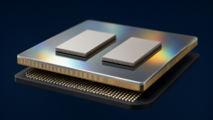
Samsung Electronics has commenced construction of a new semiconductor packaging facility at the Onyang campus in Asan, South Chungcheong Province. The facility is designed to transition the campus from conventional assembly and testing to advanced HBM packaging. Operations are scheduled to begin in June 2028, which is one year ahead of the original timeline.
Technical Details
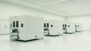
The new “fifth line” will consist of three floors providing approximately 31,000 square meters of cleanroom space. This expansion will increase the total floor area of the Onyang campus from 270,000 square meters to approximately 420,000 square meters. Samsung Electronics is allocating 46 trillion won to the Onyang HBM production lines, split between 6 trillion won for construction and 40 trillion won for the phased installation of advanced equipment.
Background & Context
This project is part of a broader 60 trillion-won commitment by Samsung Electronics across the Chungcheong provinces, including capacity expansions in Onyang and Cheonan. Furthermore, Samsung Group is executing a wider 144 trillion-won regional investment involving other affiliates:
- Samsung Display: Investing 67 trillion won in Asan and Cheonan, including 5.9 trillion won for a foldable device, laptop, and tablet OLED line targeting mass production in late 2029.
- Samsung Electro-Mechanics: Investing 8 trillion won, including 4.27 trillion won in Sejong for flip-chip ball grid array substrates for AI servers, with mass production set for September 2028.
- Samsung SDI: Investing 9 trillion won in Cheonan for next-generation battery technology and production process validation.
Significance & Outlook
The acceleration of the Onyang plant is driven by sustained demand for server memory chips. Samsung Electronics noted that while 2027 HBM supply volumes are negotiated, customers are requesting additional supplies, and shortages are expected to persist through 2028. The project is expected to create 700 jobs and generate 2.6 trillion won in economic output during construction.
Get our weekly technology intelligence — free
Receive an infographic that lets you judge at a glance whether each field’s analysis report is worth reading.
Subscribe Free — Weekly Tech Intelligence
By subscribing, you’ll receive Troy-Technical’s weekly technology intelligence newsletter.
- Your email and selected fields are used only to deliver the newsletter.
- We never share your information with third parties.
- You can unsubscribe anytime via the link in each email.
See our Privacy Policy for details.
Takes about a minute · Unsubscribe anytime